CT flat panel detector and CT machine
A technology of flat-panel detectors and operational amplifiers, which is applied in the direction of electric solid-state devices, semiconductor devices, and instruments for radiological diagnosis, etc., to achieve the effects of increasing the number of longitudinal scanning layers, good economic benefits, and reducing patient radiation
- Summary
- Abstract
- Description
- Claims
- Application Information
AI Technical Summary
Problems solved by technology
Method used
Image

Examples
Embodiment 1
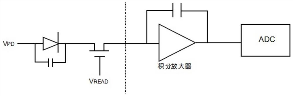
[0086] Such as Figure 4 and Figure 5 As shown, in this embodiment, the CT flat panel detector uses the junction capacitance of the photodiode itself to store and collect data, and the reading signal is added to the inside of the array element; each array element includes not only one photodiode, but also one reading Use TFT, 1 TFT for amplification and 1 TFT for reset; TFT for reading is used to control the output of data, and its control signal is called the reading signal (marked as V in each figure READ ); the reset TFT is used to reset the data, and its control signal is called a reset signal (marked as V in each figure GRST ), whose power supply is called the reset power supply (marked as V in each figure RST ); the TFT for reading is set after the TFT for amplification; in this embodiment, the post-stage operational amplifier adopts an inverting amplifier or a non-inverting amplifier. The circuit diagram of the single acquisition unit of the CT flat panel detector i...
Embodiment 2
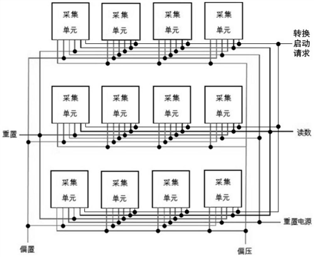
[0101] In this embodiment, the CT flat panel detector in Embodiment 1 is adopted, and the circuit diagram of each acquisition unit is as follows Figure 4 As shown, the corresponding pixel matrix circuit structure diagram is shown in Figure 5 shown. Here, the description of its structure will not be repeated.
[0102] The application condition of the CT flat panel detector in this embodiment is a CT machine adopting the working mode of the existing ray emitter: when the CT flat panel detector collects and reads, the ray emitter emits rays continuously.
[0103]Timing control in this embodiment: Since the ray emitter is still continuously emitting rays during reading, and the photodiode is constantly collecting data, for the sake of image quality, the reading time is required to be as short as possible (required reading time≤reading period 10%, the smaller the better, but the smaller the requirement for the mobility of the thin film transistor of the detector, the higher the...
Embodiment 3
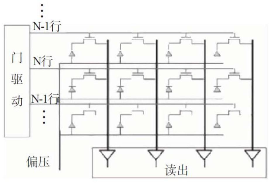
[0111] like Image 6 and Figure 7 As shown, in this embodiment, the junction capacitance of the photodiode itself is used to store and collect data; each array element in the pixel matrix includes not only a photodiode, but also a reset TFT for resetting the data , its control signal is called the reset signal, and its power source is called the reset power supply, and all array elements share the same reset power supply; the reading signal of the CT flat panel detector is input into the array element to amplify the TFT, so that the amplification is performed by the TFT Control the output of data while amplifying the process. In this embodiment, the post-stage operational amplifier is an inverting amplifier or a non-inverting amplifier.
[0112] In the CT machine of this embodiment, the ray emitter adopts the ray pulse control method in Embodiment 1, and its working principle will not be described again here.
[0113] Sequence control in this embodiment: the reading time n...
PUM
 Abstract
Description
Claims
Application Information
 - R&D
- Intellectual Property
- Life Sciences
- Materials
- Tech Scout
- Unparalleled Data Quality
- Higher Quality Content
- 60% Fewer Hallucinations
Browse by: Latest US Patents, China's latest patents, Technical Efficacy Thesaurus, Application Domain, Technology Topic, Popular Technical Reports.
© 2025 PatSnap. All rights reserved.Legal|Privacy policy|Modern Slavery Act Transparency Statement|Sitemap|About US| Contact US: help@patsnap.com