Method for forming three-dimensional structure of multi-layer conductive sheet

A technology of three-dimensional structure and forming method, applied in multilayer circuit manufacturing, 3D structure electroforming, electroforming, etc., can solve the problems of reduced feature size, high equipment requirements, and no technical solutions, etc., to achieve line hole formation The process is mild, the depth of drilling is controlled, and the effect of lowering the threshold of equipment

Active Publication Date: 2021-09-03
JIHUA LAB
View PDF4 Cites 0 Cited by
  • Summary
  • Abstract
  • Description
  • Claims
  • Application Information

AI Technical Summary

Problems solved by technology

The main driving force for this increase in integration is the continuous reduction of feature size, and more devices can be integrated in a specific area, but this is mainly in the two-dimensional direction, and the integration density cannot be further improved.
[0003] In the prior art, there are also circuit structures with some three-dimensional structures. Generally, the forming method of layer-by-layer online accumulation is adopted. Independent circuit boards are prepared by laser drilling and then welding wires or flying wires, but this method has higher requirements for equipment
[0004] For the above problems, there is no effective technical solution

Method used


Image

  • Method for forming three-dimensional structure of multi-layer conductive sheet

Examples


Embodiment 1

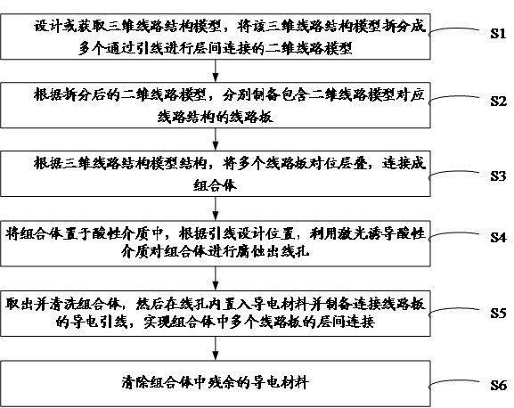
[0062] According to the use requirements, design a three-dimensional circuit structure model with a three-layer circuit structure, decompose the three-dimensional circuit structure model into three two-dimensional circuit models connected by vertical leads, and prepare three corresponding copper-containing circuit models by laser sintering. The circuit boards of high-quality circuits, the three circuit boards are connected in sequence and facing positions through glass spacers and adhesive glue to form an assembly, and the assembly is placed in the designated position of sulfuric acid solution with pH=5.2, according to the three-dimensional The position of the lead in the circuit structure model is irradiated with an ultraviolet laser with a wavelength of 357nm to heat the circuit on the circuit board, so that the temperature of the irradiation position is raised to above 50°C, and the sulfuric acid solution corrodes the circuit at the heated position to form a line hole of the ...

Embodiment 2

[0064] According to the use requirements, design a three-dimensional line structure model with a three-layer line structure, decompose the three-dimensional line structure model into three two-dimensional line models connected by vertical leads, and prepare glass blocks with openings corresponding to the positions of the leads , using laser sintering to prepare three corresponding circuit boards containing copper circuits on the glass block, and connecting the three circuit boards in sequence and facing the glass to form an assembly through adhesive glue. The assembly is placed in a designated position in a formic acid atmosphere containing water vapor, and the defect position is irradiated with an ultraviolet laser 5 with a wavelength of 357nm to heat the circuit on the circuit board, and the temperature of the irradiation position is raised to above 80°C, and the formic acid atmosphere containing water vapor Erosion the line at the heating position to form a line hole with a ...


PUM


Abstract

The invention provides a method for forming a three-dimensional structure of a multi-layer conductive sheet. The method comprises the following steps of: designing or acquiring a three-dimensional circuit structure model, and splitting the three-dimensional circuit structure model into a plurality of two-dimensional circuit models which are in interlayer connection through leads; according to the split two-dimensional circuit models, respectively preparing circuit boards comprising circuit structures corresponding to the two-dimensional circuit models; according to the structure of the three-dimensional circuit structure model, aligning and stacking the plurality of circuit boards so as to connect the circuit boards into a combined body; and placing the combined body in an acid medium, and conducting wire outgoing hole corrosion on the combined body through the acid medium induced by laser according to lead design positions. According to the forming method, the preparation process of the conductive sheet of the three-dimensional structure is effectively simplified, meanwhile, wire holes are obtained through corrosion of the acid medium induced by the laser. Compared with a traditional laser drilling mode, the wire hole forming process is milder and can effectively control the drilling depth, the focusing temperature requirement is far lower than the laser drilling temperature requirement, and the equipment threshold is effectively lowered.

Description

technical field [0001] The present application relates to the technical field of integrated circuits, in particular, to a method for forming a three-dimensional structure of multilayer conductive sheets. Background technique [0002] With the rapid development of the semiconductor industry, devices tend to be more and more miniaturized, and the number of I / Os is gradually increasing. The development trend of integrated circuits has also followed Moore's Law, and the density of integrated circuits has gradually increased. The main driving force for this increase in integration is the continuous reduction of feature size, and more devices can be integrated in a specific area, but this is mainly in the two-dimensional direction, and the integration density cannot be further improved. [0003] In the prior art, there are also circuit structures with some three-dimensional structures. Generally, the forming method of layer-by-layer online accumulation is adopted. Independent ci...

Claims


Application Information

Patent Timeline
Patent Type & Authority Applications(China)
IPC IPC(8): H05K3/46B22F10/28B22F10/62B33Y40/20C23F1/02C23F1/16C25D1/00
CPCH05K3/46H05K3/4685C23F1/02C23F1/16B22F10/62B22F10/28C25D1/003B33Y40/20Y02P10/25
Inventor 杨冠南崔成强张昱
Owner JIHUA LAB
Why Eureka
Try Eureka