Nano CMOS circuit fault-tolerant mapping method capable of optimizing power consumption

A mapping method and circuit technology, applied in the field of integrated circuits, can solve problems such as increased power consumption of nano-CMOS circuits, and achieve the effects of improving solution speed, optimizing power consumption, and reducing circuit fault tolerance complexity

Active Publication Date: 2021-09-03
NINGBO UNIV
View PDF10 Cites 0 Cited by
  • Summary
  • Abstract
  • Description
  • Claims
  • Application Information

AI Technical Summary

Problems solved by technology

[0013] The technical problem to be solved by the present invention is to provide a fault-tolerant mapping method for nano-CMOS circuits that can optimize power consumption for the problem that the defects of nano-CMOS circuits lead to increased circuit power consumption

Method used


Image

  • Nano CMOS circuit fault-tolerant mapping method capable of optimizing power consumption
  • Nano CMOS circuit fault-tolerant mapping method capable of optimizing power consumption
  • Nano CMOS circuit fault-tolerant mapping method capable of optimizing power consumption

Examples


Embodiment 1

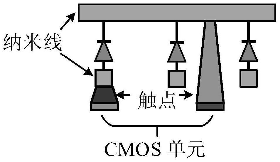
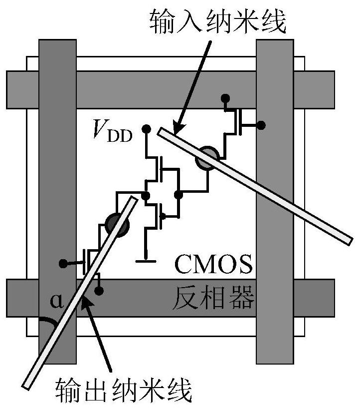
[0075] Embodiment 1: using the fault-tolerant mapping method of the present invention, the Figure 7 The logic circuit shown with 8 nodes maps to Figure 8 Defect nanoscale CMOS circuit of 4 x 4 size is shown. exist Figure 7 In the logic circuit of , there are 3 original inputs {i 1 ,i 2 ,i 3}, 3 logical nodes {g 1 , g 2 , g 3}, 2 raw outputs {o 1 ,o 2}, each node is coded according to the integer {i 1 ,i 2 ,i 3 , g 1 , g 2 , g 3 ,o 1 ,o 2}→{0,1,2,3,4,5,6,7}. exist Figure 8 In the nano-CMOS circuit of , the black dots on the nano-wires represent nano-diodes with normally connected defects. The normal nano-devices are not shown, and the units A, B, C, D, and E are normally-connected units. According to their positions in the circuit, they are From bottom to top and from left to right, it is encoded as {D,C,B,A,E}→{0,1,2,3,4}, and stored in the set P. Assuming that the radius of the connected domain is large enough, each unit is in the connected domain of e...


PUM


Abstract

The invention discloses a nano CMOS circuit fault-tolerant mapping method capable of optimizing power consumption. To solve the problem that power consumption of a circuit is increased due to the defect of a nano CMOS circuit, the method comprises the following steps of: firstly, packaging normally-connected units with higher normally-connected levels and normally-connected outputs of the normally-connected units into unit packets by packaging technology, and selecting associated nodes to generate a certain number of node packets; and completing circuit fault-tolerant mapping by a genetic algorithm, one-to-one matching mapping of a unit packet and a node packet is ensured through a specific gene coding mode and crossover and mutation operations, so that the fault-tolerant complexity is reduced, and power consumption optimization constraints are absorbed into an appropriate value function to optimize power consumption of a mapping solution. Fault-tolerant complexity of the circuit can be effectively reduced, and the power consumption optimization of the mapping circuit is realized on the basis of quickly eliminating the influence of defects on the logic function of the mapping circuit.

Description

technical field [0001] The invention relates to the field of integrated circuits, in particular to a nanometer CMOS circuit fault-tolerant mapping method capable of optimizing power consumption. Background technique [0002] As devices reach their physical limits, traditional integrated circuit technology faces many problems such as increased quantum effects and skyrocketing manufacturing costs. Researchers believe that using emerging nanoelectronic devices and corresponding nanocircuits, higher integration density and operating frequency can be obtained, thereby continuing the development of integrated circuits. Among them, the CMOS / nanowire / molecular hybrid (CMOS / nanowire / molecular hybrid, CMOL) circuit proposed by the Likharev research team of Stony Brook University in the United States is considered to be It is one of the most promising CMOS alternative technologies, and has been successfully applied in high-speed mass memory, field programmable gate array and artificia...

Claims


Application Information

Patent Timeline
Patent Type & Authority Applications(China)
IPC IPC(8): G06F30/327G06N3/12
CPCG06F30/327G06N3/126Y02D10/00
Inventor 夏银水谢尚銮查晓婧
Owner NINGBO UNIV
Why Eureka
Try Eureka