Self-rectification memristor, preparation method and application thereof
A memristor and self-rectification technology, which is applied in the field of semiconductor devices, can solve problems such as increasing the complexity of cross-array configuration, and achieve the effects of suppressing sneak current effects, improving rectification performance, and reducing power consumption
- Summary
- Abstract
- Description
- Claims
- Application Information
AI Technical Summary
Problems solved by technology
Method used
Image

Examples
Embodiment 1
[0031] This embodiment provides a method for preparing a self-rectifying memristor, comprising the following steps:
[0032] (1) Prepare the bottom electrode: place the substrate on the tray of the magnetron sputtering chamber, install the titanium nitride target on the target source of the chamber, and pump the background vacuum of the chamber to less than 2×10 -6 Torr, argon with a purity of 99.999% was introduced as the working gas, the sputtering pressure was 3mTorr, the sputtering power of the titanium nitride target was 94W, the sputtering time was 83 minutes, and the thickness was 100nm;
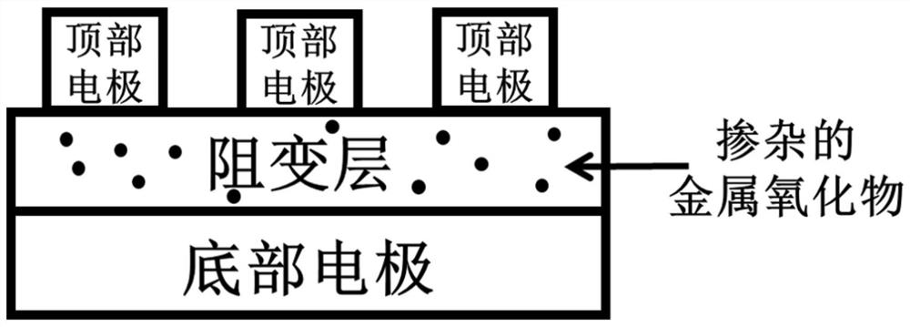
[0033] (2) Prepare the resistive layer: place the substrate on the tray of the magnetron sputtering chamber, respectively install the niobium target and the copper target on the target source of the chamber, and evacuate the background vacuum of the chamber to less than 2×10 -6 Torr, argon and oxygen are introduced as working gases, the gas flow ratio of argon and oxygen is 12:6, the...
Embodiment 2
[0042] This embodiment provides a method for preparing a self-rectifying memristor with a cross structure, comprising the following steps:
[0043] (1) Preparation of the bottom electrode: After the bottom electrode pattern is etched on the substrate, the substrate is placed on the tray of the magnetron sputtering chamber, and the tungsten target and the titanium nitride target are respectively installed on the target source of the chamber materials, and the background vacuum of the chamber is evacuated to less than 2×10 -6 Torr, argon with a purity of 99.999% is introduced as the working gas, the sputtering pressure is 3mTorr, the sputtering power of the tungsten target is 63W, the sputtering time is 5 minutes, and the thickness is 15nm; the sputtering of the titanium nitride target The power is 107W, the sputtering time is 8 minutes, and the thickness is 10nm, and a laminated bottom electrode of tungsten and titanium nitride is prepared;
[0044] (2) Prepare the resistive l...
Embodiment 3
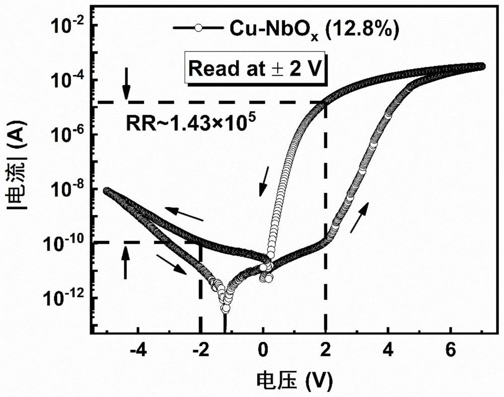
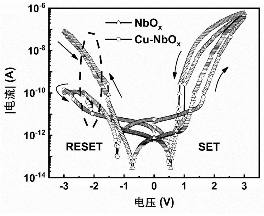
[0049] In this example, a self-rectifying memristor is prepared according to the same method as in Example 1, the difference is that the resistive layer is prepared: the substrate is placed on the tray of the magnetron sputtering chamber, on the target source of the chamber Install the niobium target and the copper target respectively, and pump the background vacuum of the chamber to less than 2×10 -6 Torr, argon and oxygen are introduced as working gases, the gas flow ratio of argon and oxygen is 12:6, the sputtering pressure is 2mTorr, copper-doped niobium oxide and niobium target are deposited by magnetron co-sputtering technology The sputtering power of the target is 141W, the sputtering time is 7 minutes, and the thickness is 20nm; the sputtering power of the copper target is 27W, the sputtering time is 7 minutes, and the thickness is 1.7nm. The calculated thickness ratio of copper doping is 7.8 %.
[0050] Figure 5 is the current-voltage (I-V) curve of the self-rectif...
PUM
| Property | Measurement | Unit |
|---|---|---|
| thickness | aaaaa | aaaaa |
Abstract
Description
Claims
Application Information
 - Generate Ideas
- Intellectual Property
- Life Sciences
- Materials
- Tech Scout
- Unparalleled Data Quality
- Higher Quality Content
- 60% Fewer Hallucinations
Browse by: Latest US Patents, China's latest patents, Technical Efficacy Thesaurus, Application Domain, Technology Topic, Popular Technical Reports.
© 2025 PatSnap. All rights reserved.Legal|Privacy policy|Modern Slavery Act Transparency Statement|Sitemap|About US| Contact US: help@patsnap.com