N-TOPCon solar cell, module and system, and method and equipment for preparing double-sided silicon oxide in cell
- Summary
- Abstract
- Description
- Claims
- Application Information
AI Technical Summary
Problems solved by technology
Method used
Image
Examples
preparation example Construction
[0058] The modification method of the equipment for preparing double-sided silicon oxide of the present invention is relatively simple and easy to implement. It is only necessary to install ion sources on both sides of the chamber body of the silicon oxide preparation process chamber and ensure uniform gas in the chamber.
[0059] In one embodiment, the positions where the carrier 132 is used to place the N-type silicon 134 are all hollowed out except for the brackets to allow the N-type silicon to be coated on both sides at the same time.
[0060] In one embodiment, the first ion source 133 is aimed downward at the front side of the N-type silicon 134 to prepare a silicon oxide film on the front side, and the second ion source 135 is aimed upward at the back side of the N-type silicon to form a silicon oxide film on the front side. Prepare a tunnel oxide layer on the front side, wherein the power of the first ion source 132 is controlled to make the thickness of the silicon ox...
Embodiment 1
[0067] A kind of N-type passivation contact structure solar cell of the present embodiment, as Figure 10 As shown, from top to bottom, it includes front p+ metal electrode 10, front SiNx passivation anti-reflection film 8, front Al 2 o 3 Passivation film 7, front silicon oxide film 3, p+ doped region 2, n-type silicon substrate 1, tunnel oxide layer 2, back n+ doped region 6, back SiNx passivation film 9, back n+ metal electrode 11.
[0068] A method for preparing a solar cell with an N-type passivation contact structure in this embodiment comprises the following steps:
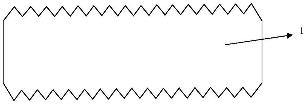
[0069] (1) Select N-type silicon 1 with a thickness of 150-170 μm, a resistivity of 0.3-2Ω·cm, and a size of 156.75mm×156.75mm as the substrate for double-sided texturing. The battery structure after this step is as follows figure 1 shown.
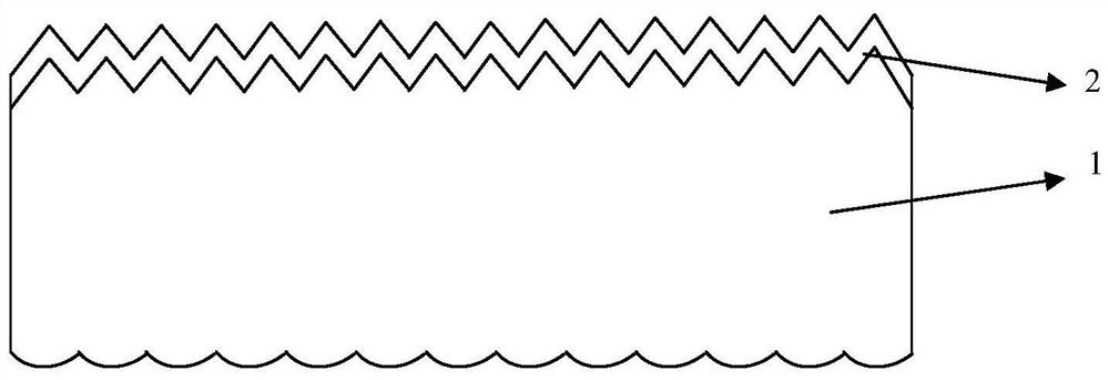
[0070] (2) Boron tribromide is used to diffuse boron on the front of the N-type silicon after the texturing treatment. The diffusion temperature is 850-1000°C, the ti...
PUM
| Property | Measurement | Unit |
|---|---|---|
| thickness | aaaaa | aaaaa |
| thickness | aaaaa | aaaaa |
| thickness | aaaaa | aaaaa |
Abstract
Description
Claims
Application Information
 - Generate Ideas
- Intellectual Property
- Life Sciences
- Materials
- Tech Scout
- Unparalleled Data Quality
- Higher Quality Content
- 60% Fewer Hallucinations
Browse by: Latest US Patents, China's latest patents, Technical Efficacy Thesaurus, Application Domain, Technology Topic, Popular Technical Reports.
© 2025 PatSnap. All rights reserved.Legal|Privacy policy|Modern Slavery Act Transparency Statement|Sitemap|About US| Contact US: help@patsnap.com


