Two-step diffusion pretreatment method for casting single-crystal or polycrystal silicon wafers

A pretreatment, silicon wafer technology, applied in the field of solar cells, can solve the problems of low minority carrier lifetime, high defect density, small angle grain boundaries, etc., to achieve the effect of retaining surface roughness, improving cell efficiency, and improving gettering effect

Pending Publication Date: 2021-07-23
XIFENG 2D FUJIAN MATERIAL TECH CO LTD
View PDF7 Cites 0 Cited by
  • Summary
  • Abstract
  • Description
  • Claims
  • Application Information

AI Technical Summary

Problems solved by technology

[0004] But casting single crystal, due to the characteristics of the casting process, there are both single crystal regions and polycrystalline regions on the same silicon wafer surface, so there are generally disadvantages such as dislocations, small-angle grain boundaries, and high defect density inside the silicon wafer. It has brought certain difficulties to the passivation of solar cells. The existing fabrication methods of cast monocrystalline silicon heterojunction solar cells are similar to the traditional heterojunction solar cell fabrication processes, even if high-quality surface cleaning and surface passivation are applied. The overall minority carrier life is still not high, which affects the conversion efficiency of the final battery

Method used


Image

  • Two-step diffusion pretreatment method for casting single-crystal or polycrystal silicon wafers
  • Two-step diffusion pretreatment method for casting single-crystal or polycrystal silicon wafers
  • Two-step diffusion pretreatment method for casting single-crystal or polycrystal silicon wafers

Examples


Embodiment Construction

[0020] The content of the present invention will be described in detail below in conjunction with the accompanying drawings and embodiments of the description:

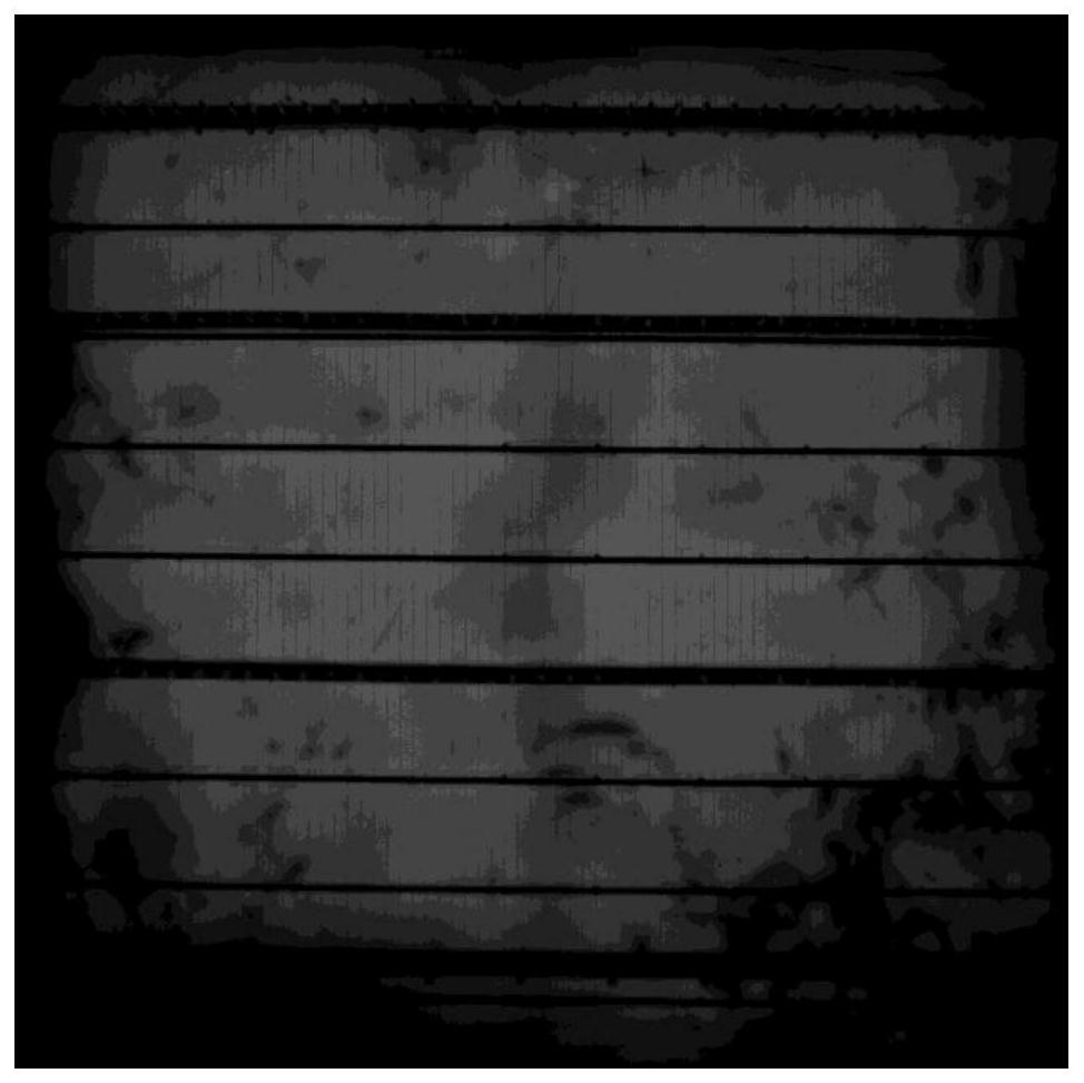
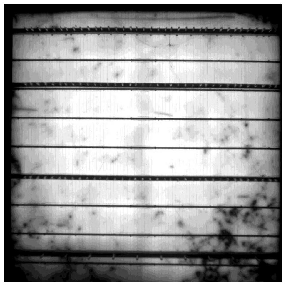
[0021] Such as Figure 2 to Figure 3 Shown is a schematic diagram of an embodiment of a two-step diffusion pretreatment method for a cast single crystal or polycrystalline silicon wafer provided by the present invention.

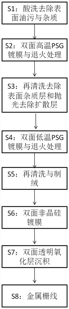
[0022] A two-step diffusion pretreatment method for casting single crystal or polycrystalline silicon wafers, it comprises the following steps,

[0023] A. Pickling: Pickling the silicon wafer with an acidic solution, then cleaning and drying;

[0024] B. Deposit PSG at high temperature: Deposit a phosphosilicate glass layer at a high temperature on the surface of the silicon wafer after the pickling treatment in step A, and perform annealing treatment;

[0025] C. One-time impurity removal: the silicon wafer after the high-temperature deposition PSG treatment in step B is cleaned and polished wit...


PUM


Abstract

The invention relates to a two-step diffusion pretreatment method for casting single-crystal or polycrystal silicon wafers, which comprises the following steps of A, pickling, B, depositing PSG at high temperature, C, primary impurity removal, D, depositing PSG at low temperature, and E, secondary impurity removal. The invention aims to provide a two-step diffusion pretreatment method for casting single-crystal or polycrystalline silicon wafers, which is suitable for effective passivation of the cast single-crystal or polycrystalline silicon wafer, and can reduce defect density in and on the surface of the silicon wafer, reduce recombination of current carriers, improve passivation level and transmission level of the current carriers, therefore, solar cell production can be carried out on the cast single-crystal or polycrystal silicon wafer according to the existing high-efficiency cell piece manufacturing process, and high cell conversion efficiency is obtained.

Description

technical field [0001] The invention relates to the field of solar cells, in particular to a two-step diffusion pretreatment method for cast single crystal or polycrystalline silicon wafers. Background technique [0002] As a new energy source, solar energy has become a vigorously developed industry in the 21st century. The research and development and production of solar cells are mainly carried out around the direction of cost reduction and efficiency increase. Improving the conversion efficiency of solar cells is the foundation of the development of solar energy business. Reducing the production cost of solar cells is the foundation of expanding the solar energy business and the prerequisite for mass production. condition. [0003] Silicon wafers are the carrier used in the production of silicon-based solar cells, generally divided into monocrystalline silicon wafers, cast monocrystalline silicon silicon wafers and polycrystalline silicon wafers. Using low-cost silicon ...

Claims


Application Information

Patent Timeline
Patent Type & Authority Applications(China)
IPC IPC(8): H01L31/18H01L31/042H01L21/322H01L21/324
CPCH01L31/1804H01L31/186H01L31/1868H01L31/1864H01L31/042H01L21/3221H01L21/324Y02P70/50Y02E10/547
Inventor 许志
Owner XIFENG 2D FUJIAN MATERIAL TECH CO LTD
Why Eureka
Try Eureka