Photoetching mask and mask pattern forming method

A photolithography mask and mask pattern technology, which is applied in the field of photolithography mask and mask pattern forming, can solve the problems of indentation of the edge of the exposure pattern, difficulty in meeting the requirements of the integrated circuit manufacturing process, etc. The effect of smoothness improvement and meeting process requirements

Pending Publication Date: 2021-07-23
泉芯集成电路制造(济南)有限公司
View PDF0 Cites 0 Cited by
  • Summary
  • Abstract
  • Description
  • Claims
  • Application Information

AI Technical Summary

Problems solved by technology

It should be noted that when the reticle obtained through this lithography process window lifting scheme is subjected to exposure processing, the exposure pattern corresponding to the sparse mask pattern usually has a relatively serious edge shrinkage phenomenon, which is not easy to meet the requirements of integrated circuits. Process requirements

Method used


Image

  • Photoetching mask and mask pattern forming method
  • Photoetching mask and mask pattern forming method
  • Photoetching mask and mask pattern forming method

Examples


Embodiment Construction

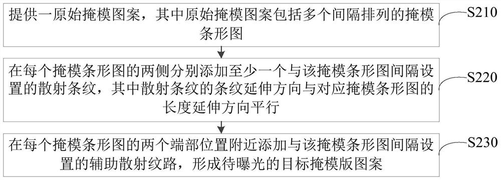
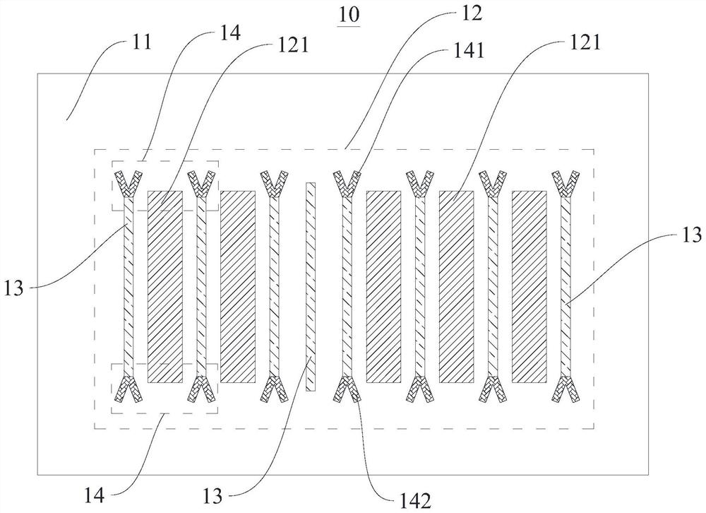
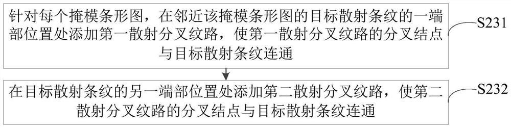
[0044] In order to make the purposes, technical solutions and advantages of the embodiments of the present application clearer, the technical solutions in the embodiments of the present application will be clearly and completely described below in conjunction with the drawings in the embodiments of the present application. Obviously, the described embodiments It is a part of the embodiments of this application, not all of them. The components of the embodiments of the application generally described and illustrated in the figures herein may be arranged and designed in a variety of different configurations.

[0045]Accordingly, the following detailed description of the embodiments of the application provided in the accompanying drawings is not intended to limit the scope of the claimed application, but merely represents selected embodiments of the application. Based on the embodiments in this application, all other embodiments obtained by persons of ordinary skill in the art wi...


PUM


Abstract

The invention provides a photoetching mask and a mask pattern forming method, and relates to the technical field of semiconductor manufacturing processes. The invention provides an original mask pattern comprising a plurality of mask bar patterns which are arranged at intervals, and at least one scattering fringe which is arranged at an interval with the mask bar pattern is added to each of the two sides of each mask bar pattern, so that the fringe extension direction of the scattering fringes is parallel to the length extension direction of the corresponding mask bar pattern; then auxiliary scattering lines which are arranged at intervals with the mask bar patterns are added near the two end parts of each mask bar pattern to form a target mask pattern to be exposed, so that when the photoetching mask with the target mask pattern is subjected to exposure treatment, the end edge smoothness of the exposure pattern obtained by exposure of the mask bar pattern can be improved through the auxiliary scattering lines, the edge shrinkage condition of the exposure pattern corresponding to the effective mask pattern is improved while the photoetching process window is improved.

Description

technical field [0001] The present application relates to the technical field of semiconductor manufacturing process, in particular, to a photolithography mask and a method for forming a pattern of the mask. Background technique [0002] With the development of integrated circuits, the size of semiconductor devices is gradually reduced, and people's demand for increasing lithography resolution and lithography process window is becoming stronger and stronger. In the process of semiconductor lithography, it is usually necessary to directly insert long strips of auxiliary scattering patterns around the sparse mask pattern, so that the sparse mask pattern can also obtain exposure conditions similar to the dense mask pattern, thereby improving the sparse mask pattern. Photolithographic process window. It should be noted that when the reticle obtained through this lithography process window lifting scheme is subjected to exposure processing, the exposure pattern corresponding to ...

Claims


Application Information

Patent Timeline
IPC IPC(8): G03F1/76
CPCG03F1/76
Inventor 孟祥鹏孙延涛陈庆煌刘志成
Owner 泉芯集成电路制造(济南)有限公司
Why Eureka
Try Eureka