
Cluster ejector pin system for semiconductor packaging die bonding

A semiconductor and thimble technology, which is applied in semiconductor/solid-state device manufacturing, electrical components, circuits, etc., can solve the problems of reducing the packaging yield, chip position deviation, and insufficient adsorption, so as to improve the stability of the die and increase the The force area and the effect of avoiding damage

Active Publication Date: 2021-07-13
湖南奥赛瑞智能科技有限公司
View PDF13 Cites 0 Cited by
  • Summary
  • Abstract
  • Description
  • Claims
  • Application Information

AI Technical Summary

Problems solved by technology

With the improvement of chip manufacturing technology, the chips produced now have been thinned from the conventional 200-300 microns to 50-120 microns. The chips of this new process can be picked up by the conventional single needle or 4 needles in the process of picking up the die bonder. damage to the chip
[0003] Similarly, when the chip bonder cooperates with the original thimble system to carry out the chip bonding operation, it is easy to cause the first adsorption not in place or the pressure is too large and too large during the bonding, so that the position of the chip will shift during the final bonding, which will affect the subsequent chip packaging. alignment of the position, reducing the package yield

Method used


Image

  • Cluster ejector pin system for semiconductor packaging die bonding
  • Cluster ejector pin system for semiconductor packaging die bonding
  • Cluster ejector pin system for semiconductor packaging die bonding

Examples


Embodiment Construction

[0025] In order to enable those skilled in the art to better understand the technical solution of the present invention, the present invention will be described in detail below in conjunction with the accompanying drawings. The description in this part is only exemplary and explanatory, and should not have any limiting effect on the protection scope of the present invention. .

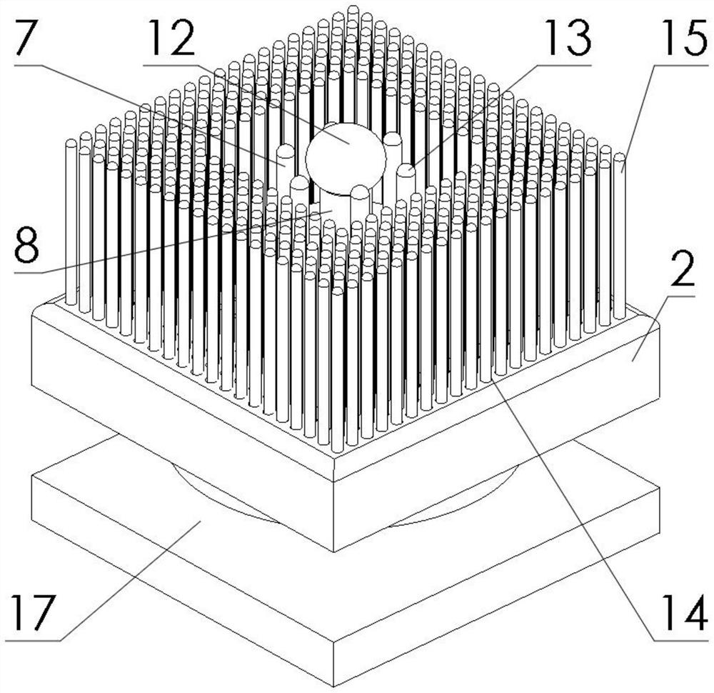
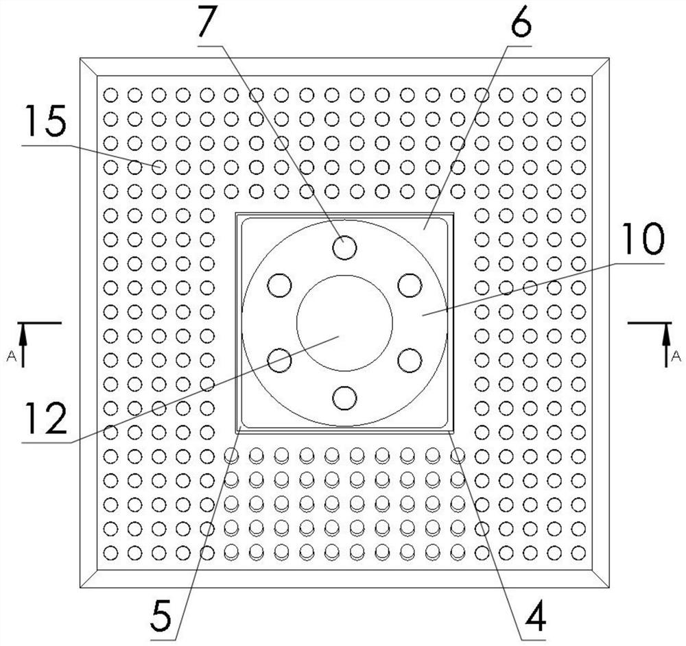
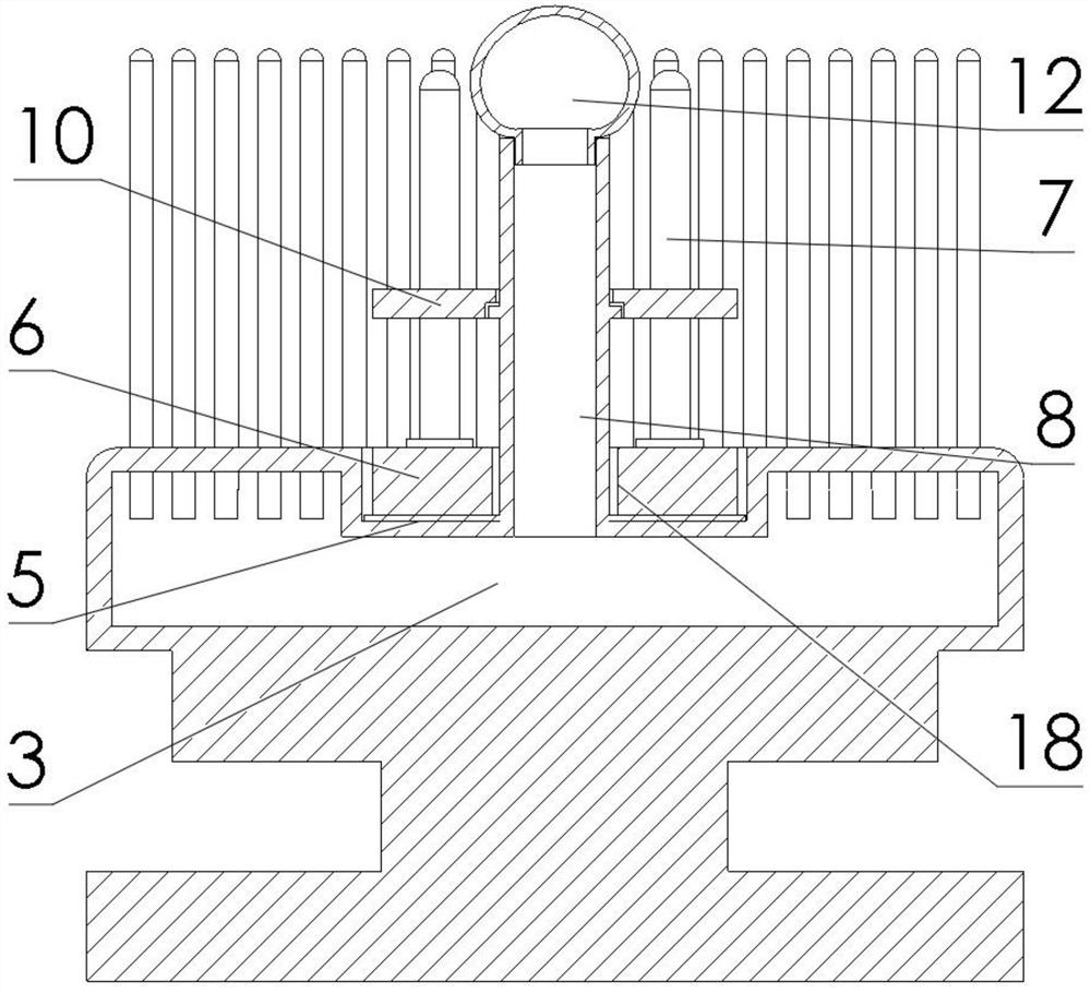
[0026] Such as Figure 1-5 As shown, the specific structure of the present invention is a cluster thimble system for semiconductor packaging adhesive chips, which is composed of a plurality of cluster thimble unit 1 arrays; the cluster thimble unit 1 includes a unit base 2, and the unit base 2 A closed air pressure cavity 3 is arranged inside; a main needle 8 is arranged vertically in the center of the unit base 2, the interior of the main needle 8 is hollow and open up and down, the top of the main needle 8 is covered with a main needle air bag 12 and In communication with it, the bottom opening of t...


PUM


Abstract

The invention discloses a cluster ejector pin system for semiconductor packaging die bonding. The cluster ejector pin system is composed of a plurality of cluster ejector pin unit arrays. Each cluster ejector pin unit comprises a unit base, and a closed air pressure cavity is formed in each unit base; a main needle is vertically arranged in the center of the unit base, the main needle is hollow and open up and down, the top of the main needle is sleeved with a main needle air bag and communicated with the main needle air bag, and a bottom opening of the main needle is communicated with the air pressure cavity; an embedding groove is formed in the center of the unit base, and a bottom plate matched with the embedding groove is arranged in the embedding groove; the center of the bottom plate is provided with a bottom plate through hole for the main needle to pass through; and a plurality of auxiliary needles are uniformly and vertically arranged around the main needle on the bottom plate at intervals in a surrounding manner, and the top of each auxiliary needle is lower than the main needle air bag and higher than the top of the main needle. According to the system disclosed by the invention, the excessive pressure of each contact point of a chip during chip bonding can be reduced through a form that the main needle is matched with the auxiliary needle and an elastic buffering main needle air bag, so that the chip is prevented from being damaged; and finally, the periphery of the chip is supported, protected, limited and positioned through the pneumatic ejector pin, so that the chip bonding stability of the central part of the chip is further improved.

Description

technical field [0001] The invention belongs to the technical field of semiconductor packaging, in particular to a cluster thimble system used for bonding chips in semiconductor packaging. Background technique [0002] In semiconductor packaging production, in the previous process of chip loading, the chip bonder uses vacuum and thimble systems to pick up chips from the blue film. The conventional process is to use one thimble for small chips and four thimbles for large chips. With the improvement of chip manufacturing technology, the chips produced now have been thinned from the conventional 200-300 microns to 50-120 microns. The chips of this new process can be picked up by the conventional single needle or 4 needles in the process of picking up the die bonder. damage to the chip. [0003] Similarly, when the chip bonder cooperates with the original thimble system to carry out the chip bonding operation, it is easy to cause the first adsorption not in place or the pressur...

Claims


Application Information

Patent Timeline
Patent Type & Authority Applications(China)
IPC IPC(8): H01L21/687H01L21/683H01L21/67
CPCH01L21/68742H01L21/6875H01L21/6838H01L21/67242Y02P70/50
Inventor 杜荣
Owner 湖南奥赛瑞智能科技有限公司
Learn More