Intermediate fixture and method for semiconductor laser failure analysis sample preparation

A failure analysis sample and laser technology, applied in the field of optical communication, can solve the problem of low sample preparation rate of semiconductor laser failure analysis samples, and achieve the effect of improving sample preparation effect, easy operation and improving grinding quality

Active Publication Date: 2022-05-20
ZHEJIANG UNIV
View PDF5 Cites 2 Cited by
  • Summary
  • Abstract
  • Description
  • Claims
  • Application Information

AI Technical Summary

Problems solved by technology

[0007] In order to solve the problem of low sample preparation rate of semiconductor laser failure analysis samples, the present invention proposes an intermediate fixture and method for semiconductor laser failure analysis sample preparation

Method used


Image

  • Intermediate fixture and method for semiconductor laser failure analysis sample preparation
  • Intermediate fixture and method for semiconductor laser failure analysis sample preparation
  • Intermediate fixture and method for semiconductor laser failure analysis sample preparation

Examples


Embodiment 1

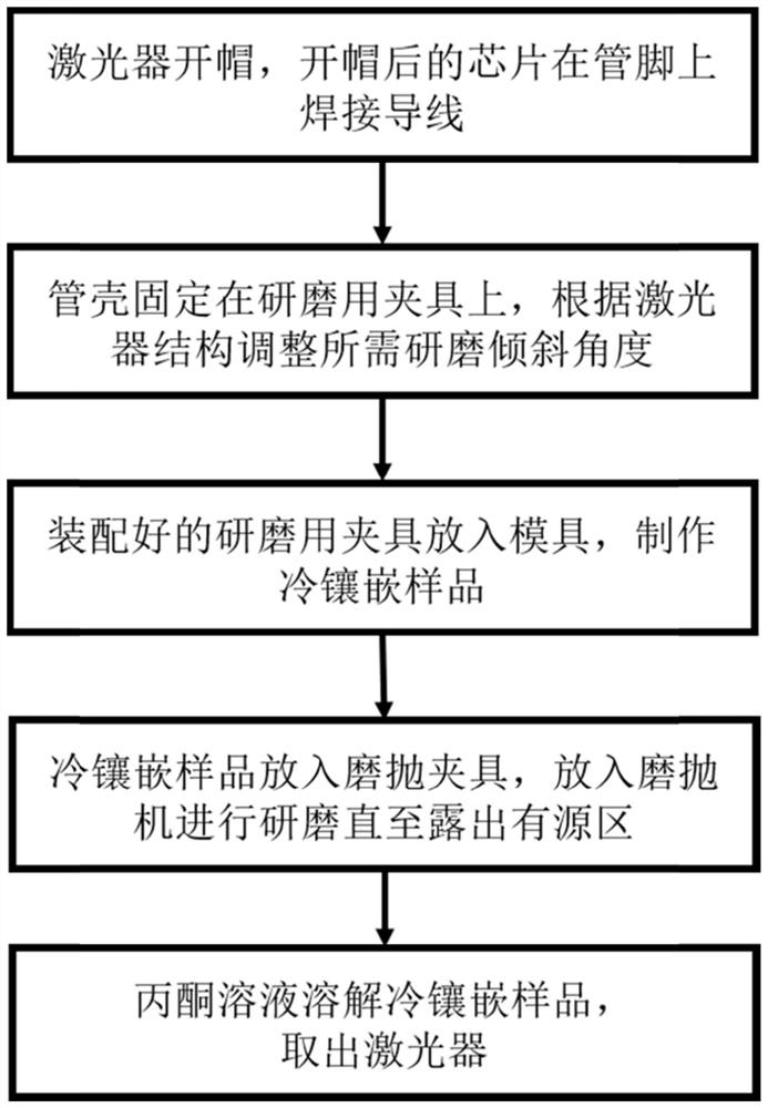
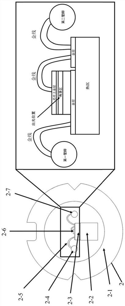
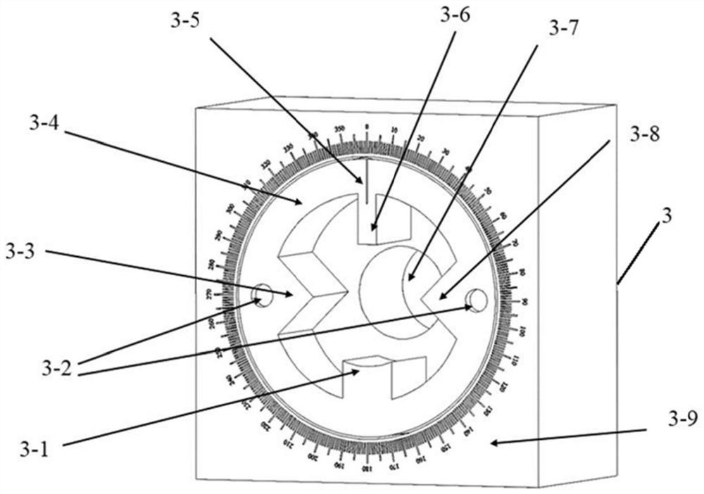
[0064] In this embodiment, the semiconductor laser failure analysis sample is prepared by the above method, wherein, since the height h=100 μm and the width W=200 μm of the TO laser, the formula 0 Figure 8 and Figure 9 shown.

[0065] The failure analysis sample of the semiconductor laser is subjected to a power-on test, that is, one end of the DC current source power supply is connected to the wire of the first pin, and the other end is added to the gold layer on the chip through a probe, and then a certain current (higher than that of the TO laser) is injected. Threshold current), the electroluminescence image of the active region is obtained, so that the effective analysis of semiconductor lasers can be realized.

Embodiment 2

[0067] This example uses the same method as in Example 1 to prepare a semiconductor laser failure analysis sample, wherein the rotation angle α' is selected as a complementary rotation angle to α in Example 1, and finally the top view of the semiconductor laser failure analysis sample obtained by grinding and dissolving and front view respectively as Figure 10 and Figure 11 shown.

[0068] The failure analysis sample of the semiconductor laser is subjected to a power-on test, that is, one end of the DC current source power supply is connected to the wire or pad of the second pin, the other end is added to the gold layer under the chip through a probe, and then a certain current (high The current at the threshold of the TO laser), the electroluminescence image of the active region is obtained, so that the effective analysis of the semiconductor laser can be realized.

[0069]The semiconductor laser failure analysis sample obtained by the intermediate fixture and method of t...


PUM

PropertyMeasurementUnit
heightaaaaaaaaaa
widthaaaaaaaaaa

Abstract

The invention discloses an intermediate fixture and a method thereof for preparing semiconductor laser failure analysis samples. The intermediate fixture includes a first clamping part and a second clamping part; the first clamping part is used to clamp a TO laser, and holds a TO The first clamping part of the laser can obtain the cold mounting sample after injection molding, and the second clamping part is used to fix the cold mounting sample and control its grinding thickness; the first clamping part includes the first shell and the cylindrical block; the second The clamping part includes a second shell, an adjusting part and a pad; the pad can move up and down under the action of the adjusting part, and at the same time adjust the size of the part of the cold mounting sample exposed to the sample groove. The preparation process of the present invention has no high-temperature operation and effectively protects the chip; at the same time, no expensive micro-nano processing equipment is required, and the sample preparation process is simple and easy to operate; the prepared samples can be directly used for electroluminescence, photoluminescence and electron beam induced current failure analysis and defect detection.

Description

technical field [0001] The invention relates to the technical field of optical communication, in particular to an intermediate fixture for preparing a semiconductor laser failure analysis sample and a method thereof. Background technique [0002] The failure analysis and defect detection methods of common lasers are electroluminescence, photoluminescence and electron beam induced current technology. Since semiconductor lasers are brittle and fragile and the chips are very small (on the order of hundreds of um), there are many samples used for failure analysis. Prepared by micro-nano processing technology. The processing cost of micro-nano processing technology is expensive, the process is complicated, and it needs to rely on large-scale process equipment in ultra-clean rooms, which limits the preparation of semiconductor laser failure analysis samples and hinders the research on the degradation mechanism of semiconductor lasers. [0003] The semiconductor laser chip is most...

Claims


Application Information

Patent Timeline
Patent Type & Authority Patents(China)
IPC IPC(8): G01N1/32G01N1/36G01N1/28G01R31/28
CPCG01N1/286G01N1/32G01N1/36G01N1/28G01R31/2898G01N2001/2866G01N2001/366
Inventor 夏明俊孙天宇
Owner ZHEJIANG UNIV
Why Eureka
Try Eureka