Semiconductor structure and forming method thereof

A semiconductor and conductive structure technology, applied in semiconductor devices, semiconductor/solid-state device manufacturing, transistors, etc., can solve the problem of small size of conductive contact window

Active Publication Date: 2021-07-06
CHANGXIN MEMORY TECH INC
View PDF12 Cites 2 Cited by
  • Summary
  • Abstract
  • Description
  • Claims
  • Application Information

AI Technical Summary

Problems solved by technology

[0005] Embodiments of the present invention provide a semiconductor structure and a method for forming the same, which help to solve the problem that the size of the conductive contact window of the semiconductor structure is too small

Method used


Image

  • Semiconductor structure and forming method thereof
  • Semiconductor structure and forming method thereof
  • Semiconductor structure and forming method thereof

Examples


Embodiment Construction

[0029] It can be seen from the background art that the size of the conductive contact window of the semiconductor structure in the prior art is too small.

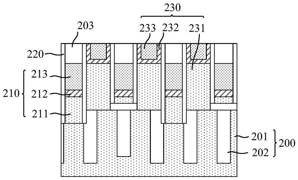
[0030] figure 1 A schematic diagram of a semiconductor structure.

[0031] refer to figure 1 , now combined with a semiconductor structure for analysis. The semiconductor structure includes: a substrate 200 and a plurality of mutually separated conductive structures 210 on the substrate; an insulating layer 203 located on the upper surface of the conductive structure; an isolation structure 220, and the isolation structure 220 is located on the sidewall of the conductive structure 210 and the side of the insulating layer 203 Wall; the surface of the substrate 200 and the sidewall of the isolation structure 220 form a trench, and in the direction perpendicular to the sidewall of the trench, the width of the opening of the trench is the same as the width of the bottom of the trench; the trench serves as a conductive contac...


PUM

PropertyMeasurementUnit
thicknessaaaaaaaaaa

Abstract

The embodiment of the invention provides a semiconductor structure and a forming method thereof. The semiconductor structure comprises the following steps: providing a substrate and a plurality of mutually separated conductive structures located on the substrate; forming an insulating layer on the upper surface of each conductive structure; forming an isolation structure, wherein the isolation structure is located on the side wall of each conductive structure and the side wall of each insulating layer; removing part of the isolation structure on the side wall of the insulating layer, wherein the upper surface of the residual isolation structure is higher than the upper surface of the conductive structure; removing part of the insulating layer away from the conductive structure, and in the direction perpendicular to the side wall of the insulating layer, the width of the top of the remaining insulating layer being smaller than that of the bottom of the remaining insulating layer; the surface of the substrate, the side wall of the isolation structure and the side wall of the insulating layer defining a groove, and the width of an opening of the groove being larger than that of the bottom of the groove in the direction perpendicular to the side wall of the groove. The embodiment of the invention is beneficial to improving the performance of the semiconductor structure.

Description

technical field [0001] Embodiments of the present invention relate to the field of semiconductors, and in particular to a semiconductor structure and a method for forming the same. Background technique [0002] Dynamic Random Access Memory (Dynamic Random Access Memory, DRAM) is a semiconductor storage device commonly used in computers, and is composed of many repeated storage units. Each memory cell usually includes a capacitor and a transistor. The gate of the transistor is connected to the word line, the drain is connected to the bit line, and the source is connected to the capacitor. The voltage signal on the word line can control the opening or closing of the transistor, and then through the bit line Read the data information stored in the capacitor, or write the data information into the capacitor through the bit line for storage. [0003] As the size of the DRAM memory cell array becomes smaller and smaller, the size of its conductive contact window is also smaller a...

Claims


Application Information

Patent Timeline
Patent Type & Authority Applications(China)
IPC IPC(8): H01L21/8242H01L27/108
CPCH10B12/30H10B12/03H10B12/482H10B12/0335H10B12/315H10B12/37H10B12/485H10B12/0387
Inventor 吴公一丁瑞艮唐贤贤邓楠王玉尘
Owner CHANGXIN MEMORY TECH INC
Why Eureka
Try Eureka