Packaging conductive structure and its manufacturing method
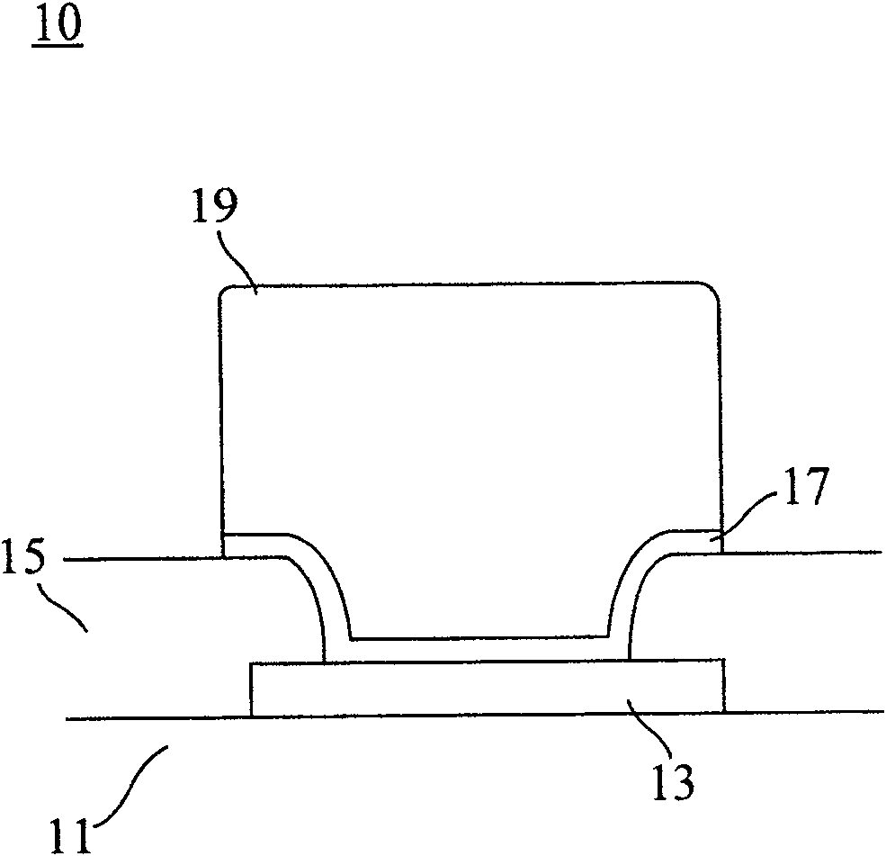
A technology of conductive structure and manufacturing method, which is applied in the direction of semiconductor/solid-state device manufacturing, circuits, electrical components, etc., and can solve problems such as open circuit, difficulty in having bonding buffer capacity, bump 19 falling off, etc.
- Summary
- Abstract
- Description
- Claims
- Application Information
AI Technical Summary
Problems solved by technology
Method used
Image
Examples
Embodiment Construction
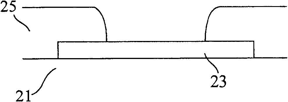
[0017] The invention discloses a packaging conductive structure for semiconductor substrates and its manufacturing method; first refer to figure 2 The semiconductor substrate 21 includes a pad 23 , which is generally made of aluminum, and serves as a contact point for the semiconductor structure inside the semiconductor substrate 21 to be electrically connected to the outside. Then, a protective layer 25 is formed on the semiconductor substrate 21, which partially covers the liner 23 to define an accommodating space; in actual manufacturing, a photoresist layer can be formed first, and then patterned. An etching process is used to remove part of the photoresist material to form an accommodating space and partially expose the liner 23 .
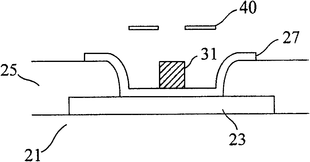
[0018] see further image 3 , forming an under bump metal layer (Under Bump Metal, UBM) 27 in the accommodation space, which is electrically connected to the pad 23 of the semiconductor substrate 21, wherein the under bump metal layer 27 is ...
PUM
 Abstract
Description
Claims
Application Information
 - R&D
- Intellectual Property
- Life Sciences
- Materials
- Tech Scout
- Unparalleled Data Quality
- Higher Quality Content
- 60% Fewer Hallucinations
Browse by: Latest US Patents, China's latest patents, Technical Efficacy Thesaurus, Application Domain, Technology Topic, Popular Technical Reports.
© 2025 PatSnap. All rights reserved.Legal|Privacy policy|Modern Slavery Act Transparency Statement|Sitemap|About US| Contact US: help@patsnap.com


