
Method for designing surface plasmon polariton wave absorber

A technology of surface plasmon and design method, which is applied in the design field of ion polariton absorbers, can solve the problems of affecting the stealth effect, destroying the scattering characteristics of antenna radiation characteristics, and enhancing the RCS of stealth objects, so as to achieve perfect absorption and realize wave impedance. The effect of matching and stable transmission

Inactive Publication Date: 2021-06-25
ZHEJIANG UNIV HANGZHOU GLOBAL SCI & TECH INNOVATION CENT
View PDF4 Cites 1 Cited by
  • Summary
  • Abstract
  • Description
  • Claims
  • Application Information

AI Technical Summary

Problems solved by technology

However, SPP signals are not always useful. Some SPP signals will destroy the radiation characteristics of antennas and the scattering characteristics of devices, especially in the stealth field. The surface excites creeping waves that propagate along the interface. This type of creeping wave reflects strongly after hitting the metal-air interface. This part of the reflection will significantly enhance the RCS of the stealth object, thereby affecting the stealth effect

Method used


Image

  • Method for designing surface plasmon polariton wave absorber
  • Method for designing surface plasmon polariton wave absorber
  • Method for designing surface plasmon polariton wave absorber

Examples


Embodiment Construction

[0039] The following will clearly and completely describe the technical solutions in the embodiments of the present invention with reference to the accompanying drawings in the embodiments of the present invention. Obviously, the described embodiments are only some, not all, embodiments of the present invention. Based on the embodiments of the present invention, all other embodiments obtained by persons of ordinary skill in the art without making creative efforts belong to the protection scope of the present invention.

[0040] An embodiment of the present invention provides a method for designing a surface plasmon wave absorber, the method comprising:

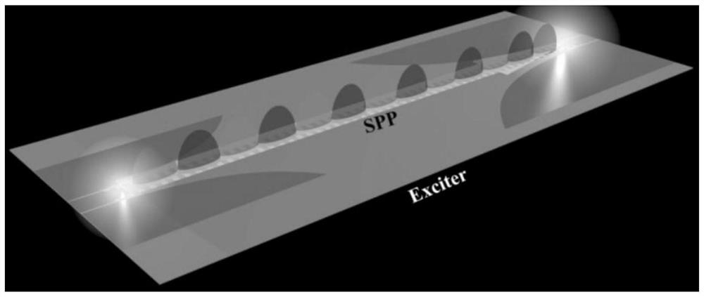
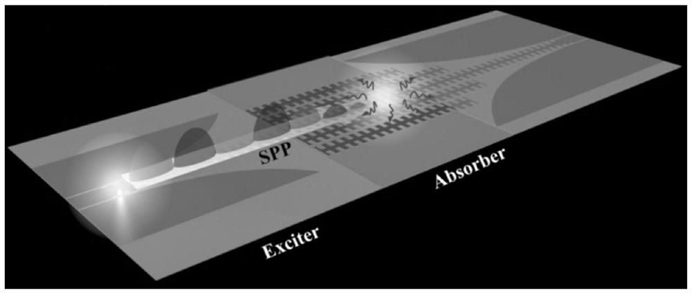
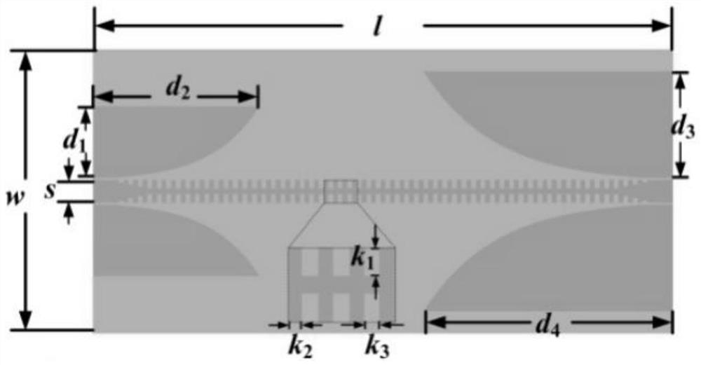
[0041] Step 1, design SPP excitation and receiver: use Vivaldi gradient slotting to generate SPP signal, couple the SPP signal to the comb-shaped eigenstructure through the coplanar waveguide CPW feeding structure, and transmit it along the comb-like eigenstructure. The end adopts the Vivaldi gradient slotting receiver.

[00...


PUM

PropertyMeasurementUnit
thicknessaaaaaaaaaa
widthaaaaaaaaaa
lengthaaaaaaaaaa

Abstract

The invention discloses a method for designing a surface plasmon polariton wave absorber, which comprises the following steps of: generating an SPP signal by adopting a Vivaldi gradually-changed slot, coupling the SPP signal to a comb-shaped intrinsic structure through a coplanar waveguide (CPW) feed structure, transmitting the SPP signal along the comb-shaped intrinsic structure, and receiving the SPP signal at a receiving end by adopting the Vivaldi gradually-changed slot. Indium tin oxide (ITO) is adopted as a basic structure of an SPP absorption unit, the wave vector of the SPP absorption unit is matched with the wave vector of an SPP signal by regulating and controlling dispersion characteristics and impedance characteristics, and the SPP absorption unit is matched with the impedance of the SPP signal; The invention is used for absorbing SPP signals in the transmission process. A broadband SPP signal is generated by adopting an SPP excitation and receiver, an SPP wave-absorbing structure is designed by adopting an indium tin oxide (ITO) structural unit, the transmission wave vector of the wave-absorbing structure is improved by adjusting the geometric dimension of ITO, so that the excited SPP signal can be stably transmitted without scattering, wave impedance matching is realized by changing the conductivity parameter of the ITO structure, and the SPP wave-absorbing structure can be applied to the field of microwave sensing. Therefore, perfect absorption of the SPP signal is realized.

Description

technical field [0001] The invention relates to the technical field of electronic information and stealth, and more specifically relates to a design method of a surface plasmon wave absorber. Background technique [0002] Surface plasmon polaritons (SPP) refer to a sub-wavelength intrinsic electromagnetic mode formed by the interference between light quanta of electromagnetic waves and free electrons in metals at the medium / metal interface. SPP has strong local field characteristics, and its electric and magnetic field amplitudes exhibit exponential decay on both sides of the interface. The unique electromagnetic properties of SPP make it have very important application value in the fields of photonics, enhanced Raman effect, optical waveguide, and plasma integrated devices. The SPP mode of the metal interface only exists in the optical frequency band, but due to the large imaginary part of the refractive index in the optical frequency band, the intrinsic SPP transmission l...

Claims


Application Information

Patent Timeline
Patent Type & Authority Applications(China)
IPC IPC(8): G06F30/20H01Q17/00
CPCG06F30/20H01Q17/00
Inventor 蔡通郑斌钱超陈红胜
Owner ZHEJIANG UNIV HANGZHOU GLOBAL SCI & TECH INNOVATION CENT
Learn More