Dry developing method based on chalcogenide phase change material GST

A technology of phase change material and development method, which is applied in the field of dry development based on chalcogenide phase change material GST, which can solve problems such as rough lines on the edges of graphics, collapse of graphics lines, and irregular shapes, so as to solve the problems of rough lines and avoid lines collapse effect

Pending Publication Date: 2021-06-22
INST OF MICROELECTRONICS CHINESE ACAD OF SCI
View PDF4 Cites 0 Cited by
  • Summary
  • Abstract
  • Description
  • Claims
  • Application Information

AI Technical Summary

Problems solved by technology

However, organic photoresists have a solvent swelling effect, which can easily lead to rough lines and irregular shapes at the edges of graphics
At the same time, the organic photoresist needs a post-baking process after development to improve the etching resistance of the photoresist, but the post-baking is easy to cause the collapse of the graphic lines, which will also lead to rough lines and irregular shapes on the edges of the graphics.

Method used


Image

  • Dry developing method based on chalcogenide phase change material GST
  • Dry developing method based on chalcogenide phase change material GST
  • Dry developing method based on chalcogenide phase change material GST

Examples


Embodiment Construction

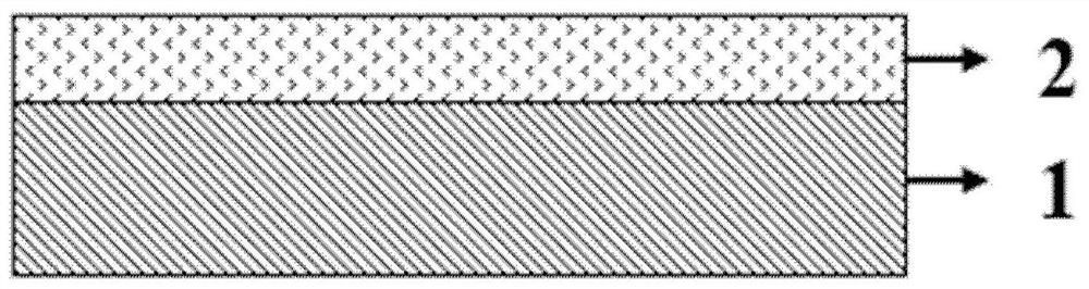
[0029] In order to make the object, technical solution and advantages of the present invention clearer, the present invention will be further described in detail below in conjunction with specific embodiments and with reference to the accompanying drawings.

[0030] It should be understood, however, that these descriptions are exemplary only and are not intended to limit the scope of the present invention. In the following detailed description, for purposes of explanation, numerous specific details are set forth in order to provide a thorough understanding of the embodiments of the invention. It may be evident, however, that one or more embodiments may be practiced without these specific details. In addition, in the following description, descriptions of known technologies are omitted to avoid unnecessarily confusing the concept of the present invention.

[0031] The terminology used herein is for the purpose of describing particular embodiments only, and is not intended to b...


PUM

PropertyMeasurementUnit
thicknessaaaaaaaaaa

Abstract

The invention discloses a dry development method based on a chalcogenide phase change material GST. The dry development method comprises the following steps: depositing a layer of Ge2Sb2Te5 film on a substrate; performing direct-writing exposure on the Ge2Sb2Te5 thin film by using an electron beam according to a preset pattern, so that the material characteristic of an exposure region of the Ge2Sb2Te5 thin film is converted from an amorphous state to a crystalline state, and the material characteristic of a non-exposure region of the Ge2Sb2Te5 thin film is kept in the amorphous state; etching the Ge2Sb2Te5 thin film by using an inductively coupled plasma to form a preset pattern, wherein the etching speed of a crystalline region in the Ge2Sb2Te5 thin film is higher than that of an amorphous region of the Ge2Sb2Te5 thin film. According to the invention, the characteristic that the material characteristics of the Ge2Sb2Te5 thin film are variable is utilized, the Ge2Sb2Te5 thin film presents regions with different etching speeds through electron beams, so that step-shaped patterns are formed on the Ge2Sb2Te5 thin film in the inductively coupled plasma etching stage, dry development is achieved, and the etching speed of the Ge2Sb2Te5 thin film is improved. The problem of line collapse is avoided, and the problems of rough pattern edge lines and irregular shapes are solved.

Description

technical field [0001] The invention relates to the technical field of micro-nano processing, in particular to a dry developing method based on chalcogenide phase change material GST. Background technique [0002] The traditional image transfer method adopts the wet developing technology of organic photoresist. However, organic photoresists have a solvent swelling effect, which can easily lead to rough lines and irregular shapes at the edges of graphics. At the same time, the organic photoresist needs a post-baking process after development to improve the etching resistance of the photoresist, but the post-baking is easy to cause the collapse of the graphic lines, which will also lead to rough lines and irregular shapes on the edges of the graphics. Contents of the invention [0003] Chalcogenide Phase Change Material Ge 2 Sb 2 Te 5 (GST for short) is a ternary compound with good non-volatility and high stability, and has a wide range of applications in next-generation...

Claims


Application Information

Patent Timeline
Patent Type & Authority Applications(China)
IPC IPC(8): G03F7/26G03F7/42G03F7/004
CPCG03F7/26G03F7/427G03F7/0043
Inventor 何佩谣谢常青朱效立牛洁斌叶甜春
Owner INST OF MICROELECTRONICS CHINESE ACAD OF SCI
Why Eureka
Try Eureka