Display substrate, manufacturing method thereof and display device

A technology for a display substrate and a manufacturing method, which is used in the manufacture of semiconductor/solid-state devices, electrical components, and electrical solid-state devices, etc., can solve problems such as long alignment time, inability to guarantee the position and size accuracy of functional graphics, and achieve guaranteed accuracy. , the overall time shortening, the effect of shortening the exposure time

Pending Publication Date: 2021-06-18
WUHAN BOE OPTOELECTRONICS TECH CO LTD +1
View PDF0 Cites 0 Cited by
  • Summary
  • Abstract
  • Description
  • Claims
  • Application Information

AI Technical Summary

Problems solved by technology

[0003] The more accurate the alignment, the longer the alignment time will be, and even if the alignment is accurate, sometimes the accuracy of the position and size of the formed functional graphics cannot be guaranteed

Method used


Image

  • Display substrate, manufacturing method thereof and display device
  • Display substrate, manufacturing method thereof and display device
  • Display substrate, manufacturing method thereof and display device

Examples


Embodiment Construction

[0047] In order to further illustrate the display substrate, the manufacturing method thereof, and the display device provided by the embodiments of the present invention, a detailed description will be given below in conjunction with the accompanying drawings.

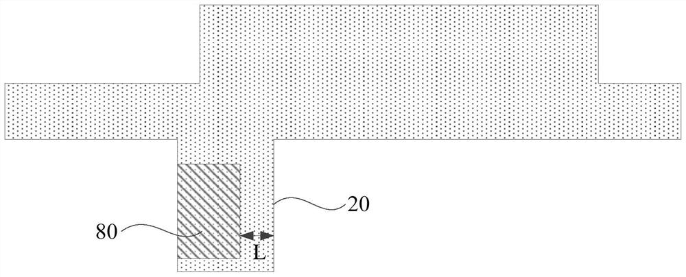
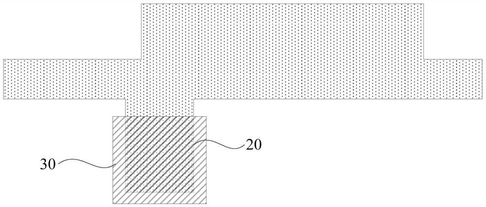
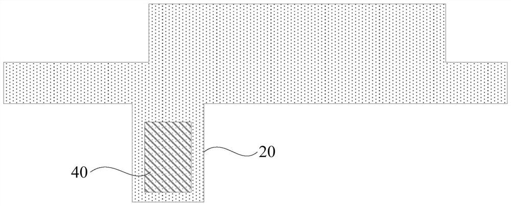
[0048] Such as figure 1 As shown, in the related art, when making the functional pattern 80, it can be formed by a patterning process, which specifically includes: depositing and forming a functional layer on the substrate; forming a photoresist layer on the side of the functional layer facing away from the substrate, The photoresist layer is subjected to an exposure process and a development process to form a photoresist pattern, and then the functional layer is etched to form a functional pattern by using the photoresist pattern as a mask.

[0049] When performing an exposure process on the photoresist layer, it is necessary to precisely align the photoresist layer with the mask plate, so as to ensure the precision ...


PUM


Abstract

The invention provides a display substrate, a manufacturing method thereof and a display device, relates to the technical field of display, and aims to shorten the manufacturing time of a functional graph while ensuring the manufacturing precision of the functional graph in a display device. The manufacturing method of the display substrate comprises the following steps: manufacturing a shading pattern on a light-transmitting substrate; manufacturing a functional layer at the side, back on to the light-transmitting substrate, of the shading pattern; manufacturing a photoresist transition pattern on one side, opposite to the light-transmitting substrate, of the functional layer; taking the shading pattern as a mask, and performing a back exposure process on the photoresist transition pattern at the side, back to the photoresist transition pattern, of the light-transmitting substrate; performing a developing process on the photoresist transition pattern subjected to the back exposure process to form a photoresist target pattern; and patterning the functional layer by taking the photoresist target pattern as a mask to form a functional pattern. The manufacturing method provided by the invention is used for manufacturing the display substrate.

Description

technical field [0001] The invention relates to the field of display technology, in particular to a display substrate, a manufacturing method thereof, and a display device. Background technique [0002] With the continuous development of display technology, the application fields of display devices are becoming more and more extensive. The display device includes a variety of functional graphics, and the functional graphics are generally formed through a patterning process. The patterning process includes forming a photoresist on the functional graphics to be formed, and performing an exposure process on the photoresist. When performing the exposure process , accurate alignment is required to ensure the precise size and position of the subsequently formed functional graphics and ensure the display performance of the display device. [0003] The more accurate the alignment, the longer the alignment time is required, and even if the alignment is accurate, sometimes the accura...

Claims


Application Information

Patent Timeline
IPC IPC(8): H01L21/027H01L21/84H01L23/544H01L27/12
CPCH01L27/1288H01L27/1218H01L27/1262H01L23/544H01L21/0274
Inventor 尹雄宣
Owner WUHAN BOE OPTOELECTRONICS TECH CO LTD
Why Eureka
Try Eureka