
Silicon optical chip temperature sensor

A temperature sensor and silicon photonic chip technology, applied in the field of optical communication, can solve the problems of complex data processing, high light source requirements, large size, etc., and achieve the effect of high overall integration, high reliability, and reduced requirements

Pending Publication Date: 2021-06-18
武汉科宇智联信息技术有限公司
View PDF0 Cites 0 Cited by
  • Summary
  • Abstract
  • Description
  • Claims
  • Application Information

AI Technical Summary

Problems solved by technology

Its devices include frequency-sweeping lasers, optical fiber beam splitters, optical fiber circulators, optical fiber couplers, photodetectors, and data acquisition cards. The entire system is large in size, complex in data processing, and high in cost.
Another built-in silicon optical chip temperature sensor is composed of import / export silicon waveguide and micro-ring waveguide. The optical signal is imported from the silicon waveguide, some optical signals of specific wavelengths are coupled into the micro-ring waveguide, and the rest of the optical signals are exported from the same silicon waveguide. , its disadvantage is that it has high requirements on the light source and must be a light source that works in a specific wavelength range

Method used


Image

  • Silicon optical chip temperature sensor
  • Silicon optical chip temperature sensor
  • Silicon optical chip temperature sensor

Examples


Embodiment Construction

[0023] The principles and features of the present invention are described below in conjunction with the accompanying drawings, and the examples given are only used to explain the present invention, and are not intended to limit the scope of the present invention.

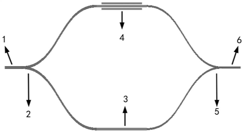
[0024] Such as figure 1 The silicon photonic chip temperature sensor shown is set in the silicon photonic chip, based on the Mach-Zehnder structure, including an input waveguide 1 with a silicon dioxide cladding, a Y-shaped waveguide 2, a first sensing waveguide 3, The second sensing waveguide 4 , the derived Y-shaped waveguide 5 and the output waveguide 6 . The input end of the input waveguide 1 receives an optical signal input, the output end of the input waveguide 1 is connected to the input end of the Y-shaped waveguide 2, and an output end of the Y-shaped waveguide 2 passes through the first transmission The sensing waveguide 3 is connected to one input end of the deriving Y-shaped waveguide 5, and the other o...


PUM

PropertyMeasurementUnit
widthaaaaaaaaaa
lengthaaaaaaaaaa

Abstract

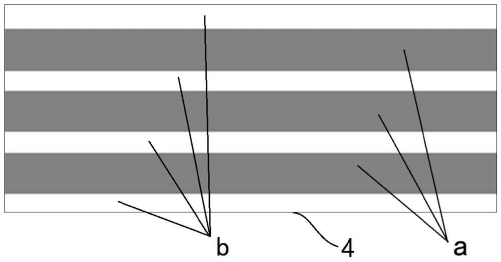
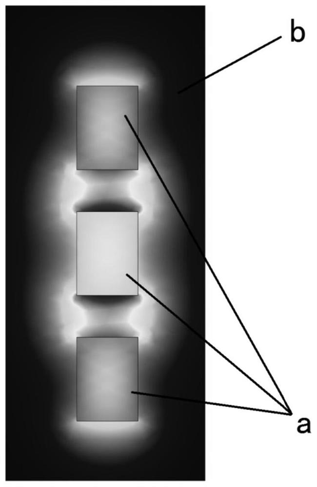
The invention relates to a silicon optical chip temperature sensor, which comprises an input waveguide provided with a silicon dioxide cladding, a lead-in Y-shaped waveguide, a first sensing waveguide, a second sensing waveguide, a lead-out Y-shaped waveguide and an output waveguide; the input waveguide is connected with the input end of the lead-in Y-shaped waveguide; the two output ends of the lead-in Y-shaped waveguide are respectively connected in series with the first sensing waveguide and the second sensing waveguide and then are respectively connected with the two input ends of the lead-out Y-shaped waveguide, and the output end of the lead-out Y-shaped waveguide is connected with the output waveguide; the second sensing waveguide comprises three silicon waveguides which are tightly arranged side by side, and two ends of the silicon waveguide positioned in the middle are respectively connected with a lead-in Y-shaped waveguide and a lead-out Y-shaped waveguide; wherein in the first sensing waveguide, an optical signal is bound to be propagated in the silicon waveguide; and in the second sensing waveguide, the optical signal is bound to be propagated in the silicon dioxide cladding between the adjacent silicon waveguides. According to the temperature sensor, temperature detection of the built-in integrated silicon optical chip is realized, and the reliability is high.

Description

technical field [0001] The invention relates to the technical field of optical communication, in particular to the technical field of silicon photonic chips, and in particular to a silicon photonic chip temperature sensor. Background technique [0002] Silicon photonics chips have the advantages of small size, high bandwidth, and low power consumption, and have great application prospects in the field of optical communications, including various environments such as data centers and the Internet of Things. However, silicon has a high thermal-optic coefficient, so the optical characteristics of silicon photonic chips are quite different under different temperature environments. Therefore, in order to ensure the working stability of silicon photonic chips, it is necessary to control the temperature of silicon photonic chips monitor. At present, silicon photonic chip temperature sensors can be divided into two categories, including external temperature sensors and built-in tem...

Claims


Application Information

Patent Timeline
Patent Type & Authority Applications(China)
IPC IPC(8): G01K11/00
CPCG01K11/00
Inventor 郑宇黄颖
Owner 武汉科宇智联信息技术有限公司
Learn More