Driving backboard and manufacturing method thereof

A technology for driving backplanes and manufacturing methods, which is applied to electrical components, circuits, semiconductor devices, etc., and can solve problems such as short circuits between driving backplanes and LED chips, and achieve the effect of preventing adhesion and reducing short-circuit problems

Inactive Publication Date: 2021-06-15
CHONGQING KONKA PHOTOELECTRIC TECH RES INST CO LTD
View PDF12 Cites 3 Cited by
  • Summary
  • Abstract
  • Description
  • Claims
  • Application Information

AI Technical Summary

Problems solved by technology

[0005] In view of the deficiencies in the prior art above, the purpose of the present invention is to provide a driving backplane and its manufacturing method, aiming to solve the problem of short circuit in the bonding process between the driving backplane and LED chips

Method used


Image

  • Driving backboard and manufacturing method thereof
  • Driving backboard and manufacturing method thereof
  • Driving backboard and manufacturing method thereof

Examples


Embodiment Construction

[0038] In order to enable those skilled in the art to better understand the solutions of the present invention, the technical solutions in the embodiments of the present invention will be clearly and completely described below in conjunction with the drawings in the embodiments of the present invention. Obviously, the described embodiments are only It is a part of embodiments of the present invention, but not all embodiments. Based on the embodiments of the present invention, all other embodiments obtained by persons of ordinary skill in the art without making creative efforts belong to the protection scope of the present invention.

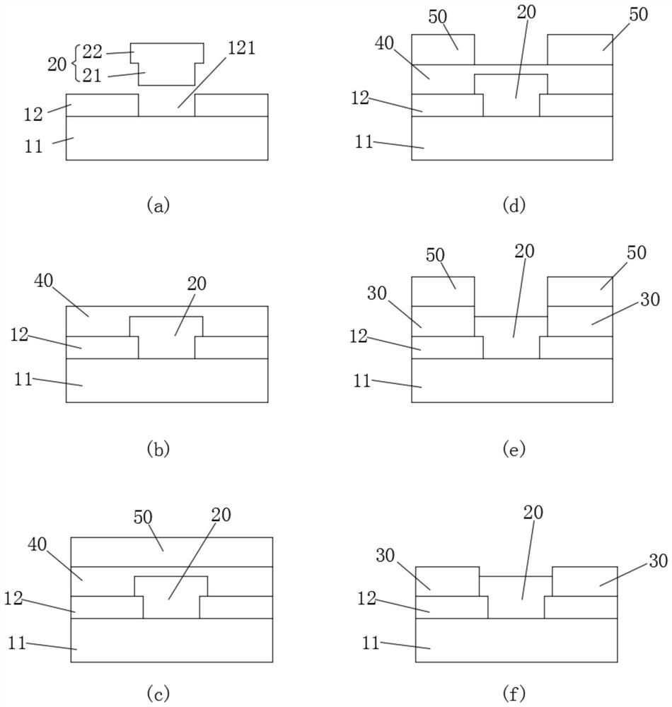
[0039] At present, as a new generation of display technology, Micro LED technology has higher brightness, better luminous efficiency, and lower power consumption than the existing Organic Light-Emitting Diode (OLED) technology, and is more worthy of promotion and application. The implementation method of Micro LED technology is to first grow flip...


PUM


Abstract

The invention discloses a driving backboard and a manufacturing method thereof. The driving backboard comprises a substrate, a convex point lower metal layer and a microstructure layer; the bump lower metal layer is arranged on the substrate and is used for butt joint with an LED chip; the microstructure layer is arranged on the substrate and is attached to the side wall of the bump lower metal layer; and the upper surface of the microstructure layer is higher than the upper surface of the bump lower metal layer. When the driving backboard is installed, the LED chip is in butt joint with the under bump metal layer, the electrodes of the LED chip and the under bump metal layer are wrapped by the microstructure layer in the bonding process, flowing of bonding metal in a molten state is limited, and short circuit problems on the driving backboard are reduced.

Description

technical field [0001] The invention relates to the technical field of display devices, in particular to a driving backplane and a manufacturing method thereof. Background technique [0002] With the advancement of display technology, display devices increasingly need display panels with higher brightness, better luminous efficiency, and lower power consumption to meet people's needs, so Micro LED (Light Emitting Diode, light emitting diode) chip technology Such a new generation of chip technology has a good development prospect. In Micro LED chip technology, a large number of micron-scale light-emitting diode chips are grown on a growth substrate, and then these light-emitting diode chips are transferred and bonded to the driver backplane through mass transfer to complete the manufacturing process. The corresponding driver Several under-bump metal layers are arranged on the back plate to be bonded to the electrodes of the light-emitting diode chips. [0003] However, duri...

Claims


Application Information

Patent Timeline
Patent Type & Authority Applications(China)
IPC IPC(8): H01L33/48H01L33/62
CPCH01L33/62H01L33/483H01L2933/0033H01L2933/0066
Inventor 范春林王斌汪庆萧俊龙汪楷伦
Owner CHONGQING KONKA PHOTOELECTRIC TECH RES INST CO LTD
Why Eureka
Try Eureka