MTJ device
A device and reference layer technology, applied in the direction of magnetic field-controlled resistors, material selection, etc., can solve the problems of large write current, small write current, read disturbance device stability, etc., to reduce critical current and write The effect of current
- Summary
- Abstract
- Description
- Claims
- Application Information
AI Technical Summary
Problems solved by technology
Method used
Image
Examples
Embodiment 1
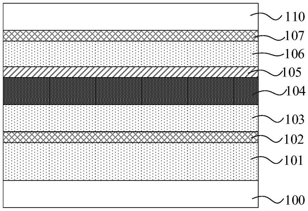
[0029] An embodiment of the present invention provides an MTJ device, such as figure 1 As shown, it includes a bottom electrode 100, a top electrode 110, and a stacked structure between the bottom electrode 100 and the top electrode 110. The material of the bottom electrode 100 is selected from Ta, Pt, W, Cu, Ti, TiN, TaN and Ru. Any one, the material of the top electrode 110 is selected from any one of Ta, Al, Cu, Ti, TiN, TaN and Ru. The laminated structure includes: a reference layer 101, a barrier layer 102, a free layer 103, an antiferromagnetic layer 104, a first coupling layer 105, a spin polarized layer 106 and a covering layer 107 stacked in sequence from bottom to top, wherein ,
[0030] The reference layer 101 has a fixed magnetization approximately perpendicular to the plane of the reference layer 101; the free layer 103 has a magnetization approximately perpendicular to the plane of the free layer 103 and the magnetization direction can be approximately parallel ...
Embodiment 2
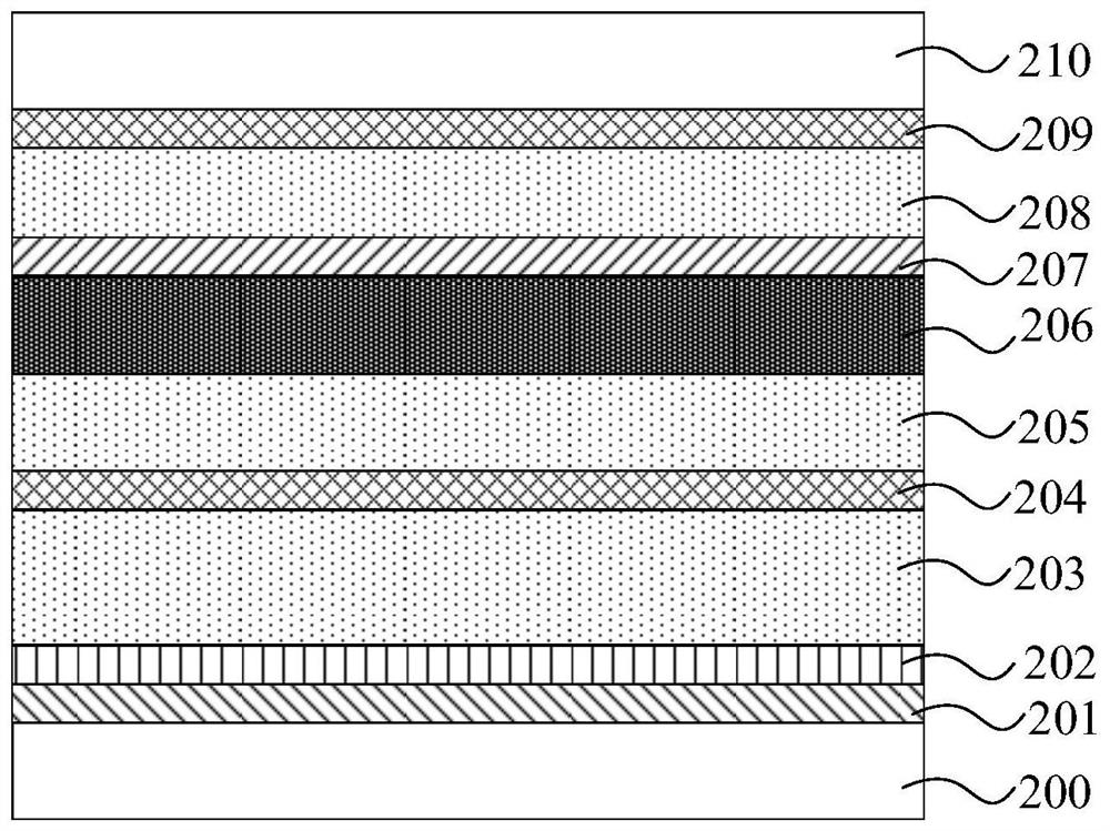
[0041] Another embodiment of the present invention provides an MTJ device, such as figure 2 As shown, it includes a bottom electrode 200, a top electrode 210, and a stacked structure between the bottom electrode 200 and the top electrode 210. The material of the bottom electrode 200 is selected from Ta, Pt, W, Cu, Ti, TiN, TaN and Ru. Any one, the material of the top electrode 210 is selected from any one of Ta, Al, Cu, Ti, TiN, TaN and Ru. The stacked structure includes: a pinned layer 201, a second coupling layer 202, a reference layer 203, a barrier layer 204, a free layer 205, an antiferromagnetic layer 206, a first coupling layer 207, a self- spin polarized layer 208 and cover layer 209, wherein,
[0042] The reference layer 203 has a fixed magnetization approximately perpendicular to the plane of the reference layer 203; the free layer 205 has a magnetization approximately perpendicular to the plane of the free layer 205 and the magnetization direction may be approximate...
PUM
 Abstract
Description
Claims
Application Information
 - R&D
- Intellectual Property
- Life Sciences
- Materials
- Tech Scout
- Unparalleled Data Quality
- Higher Quality Content
- 60% Fewer Hallucinations
Browse by: Latest US Patents, China's latest patents, Technical Efficacy Thesaurus, Application Domain, Technology Topic, Popular Technical Reports.
© 2025 PatSnap. All rights reserved.Legal|Privacy policy|Modern Slavery Act Transparency Statement|Sitemap|About US| Contact US: help@patsnap.com


