Self-luminous display panel and method of manufacturing self-luminous display panel
A display panel and self-luminous technology, which is applied in semiconductor/solid-state device manufacturing, diodes, organic semiconductor devices, etc., can solve problems such as degradation, and achieve the effect of suppressing uneven viewing angles
- Summary
- Abstract
- Description
- Claims
- Application Information
AI Technical Summary
Problems solved by technology
Method used
Image
Examples
Embodiment approach
[0085] Next, a self-emitting display panel according to a manner of the present invention will be described with reference to the drawings by a top emission type organic EL display panel. In addition, the drawings include schematic diagrams, there is a case where the scales, vertical and horizontal ratios, or the like are different.
no. 1 approach >
[0087] 1. Composition of the organic EL display panel 100
[0088] 1.1 constitutes an overview
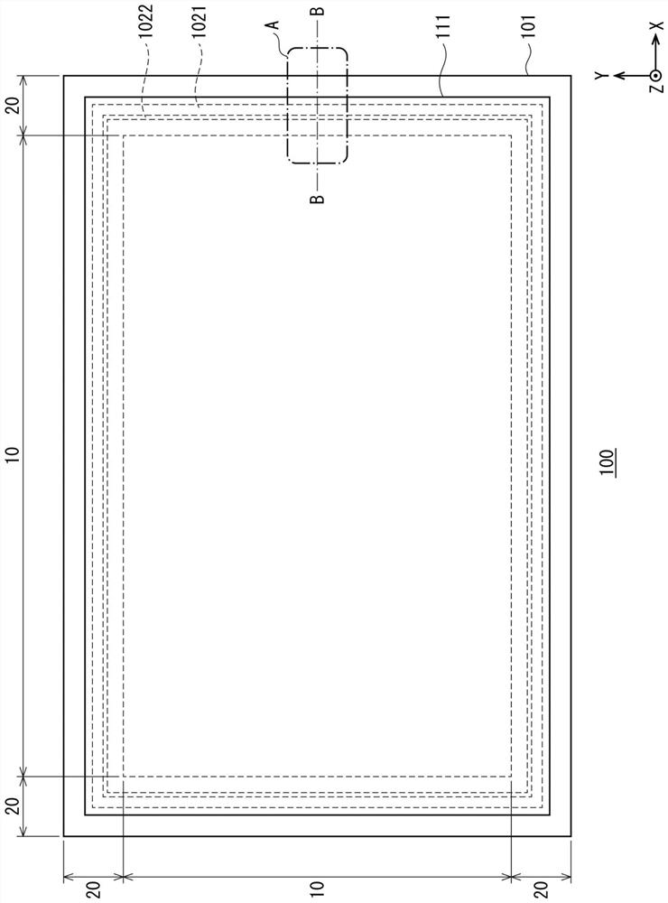
[0089] figure 1 It is a planar layout of the organic EL display panel 100 of the first embodiment.
[0090] As shown in the figure, the organic EL display panel 100 has an image display region 10 in a plan view and a peripheral region 20 around the image display area 10.
[0091] A plurality of pixels are arranged in a matrix in the image display area 10. Each pixel includes a plurality of sub-pixels having a color, in the present embodiment, the pixels include red sub-pixels, green sub-pixels, and blue sub-pixels. One sub-pixel is formed from one organic EL element.
[0092] Further, a plurality of terminals (not shown) for electrically connecting to the external driving circuit are disposed in the peripheral region 20.
[0093] 1.2 Macroable Structure of Organic EL Display Panel 100
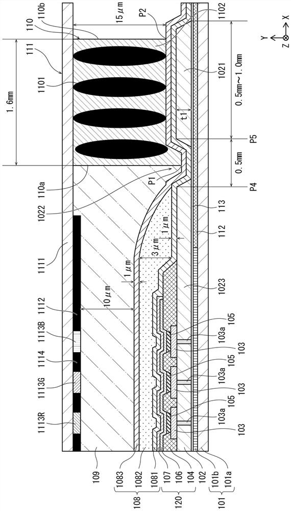
[0094] figure 2 It is a partial cross-sectional view showing the laminated structure of the outer p...
no. 2 approach >
[0213] In the first embodiment, the resin material of the second sealing layer 1082 stops the wetting spread of the wetting spread show in the inner side of the inner peripheral portion of the circumferential groove 1022. (Refer to the reference) figure 2 ), Depending on the change in the temperature and the like, the slight change of the ink concentration, the viscosity of the type of ink material, etc., such as Figure 9 As shown, there may be a case where the peripheral portion of the second sealing layer 1082 enters the circumferential groove 1022. However, since the outer insulating layer 1021 functions as a dam, the peripheral portion of the second sealing layer 1082 does not cross the end surface of the inside of the outer insulating layer 1021 and extends to the outer side (flat portion of the outer insulating layer 1021). ).
[0214] In addition, in Figure 9 In the thickness direction, the magnification is exaggerated, but in practice, the thickness of the sealing layer 10...
PUM
 Abstract
Description
Claims
Application Information
 - R&D
- Intellectual Property
- Life Sciences
- Materials
- Tech Scout
- Unparalleled Data Quality
- Higher Quality Content
- 60% Fewer Hallucinations
Browse by: Latest US Patents, China's latest patents, Technical Efficacy Thesaurus, Application Domain, Technology Topic, Popular Technical Reports.
© 2025 PatSnap. All rights reserved.Legal|Privacy policy|Modern Slavery Act Transparency Statement|Sitemap|About US| Contact US: help@patsnap.com


