Ultraviolet band ultra-low absorption double-sided antireflection film and preparation method thereof
A technology of ultraviolet band and anti-reflection coating, which is applied in the direction of optical components, optics, instruments, etc., can solve the problems that the service life and use effect of the lens cannot meet the customer's requirements, and the film layer has large absorption.
- Summary
- Abstract
- Description
- Claims
- Application Information
AI Technical Summary
Problems solved by technology
Method used
Image
Examples
Embodiment 1
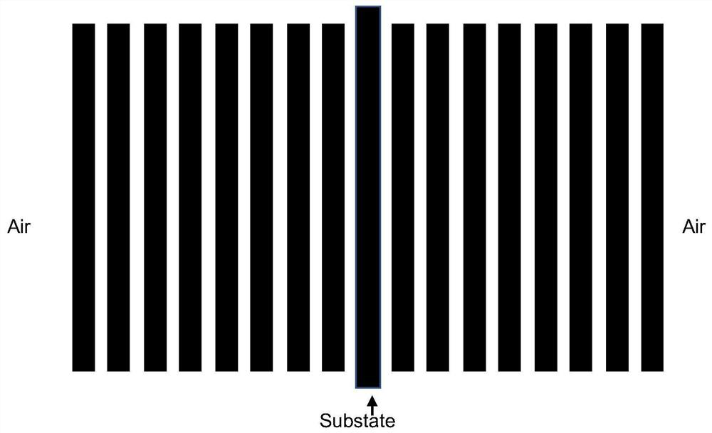
[0040] Such as figure 1 As shown, a double-sided anti-reflection coating with ultra-low absorption in the ultraviolet band has a structure of Air / LHLHLHLH / Sub / HLHLHLHL / Air, where H represents SiO 2 Film layer, the thickness is 63mm, L stands for MgF 2 The film layer has a thickness of 60mm, Sub represents the substrate, the thickness of the substrate is 5mm, and the material is fused silica.
[0041] The preparation method of above-mentioned antireflection film, comprises the steps:
[0042] (1) Substrate heating: Wipe the substrate with a degreasing gauze dipped in a 3:1 mixture of absolute ethanol and ether, then use ultrasonic cleaning to clean the substrate, and then bake and heat the substrate in a vacuum state to increase the temperature of the substrate. Wherein, the baking temperature is 160°C-170°C, and the baking time is 1.5 hours;
[0043] (2) Ion beam cleaning: perform ion beam cleaning on the substrate, the ion cleaning time is 2min, the ion beam voltage is 100...
Embodiment 2
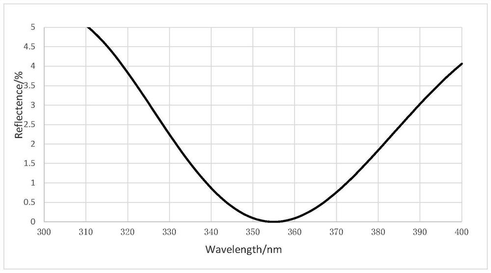
[0053] Such as figure 2 As shown, a double-sided anti-reflection film with ultra-low absorption in the ultraviolet band has a structure of: Air / 1.06L0.63H1.27L0.66H / Sub / 0.66H1.27L0.63H1.06L / Air, and the theoretical thickness of each layer is 36.84 / 81.84 / 35.17 / 68.3 / Sub / / 68.3 / 35.17 / 81.84 / 36.84nm, where H stands for LaF 3 film layer, L stands for AlF 3 For the film layer, Sub represents the substrate, the thickness of the substrate is 5mm, and the material is sapphire.
[0054] The preparation method of above-mentioned antireflection film, comprises the steps:
[0055] (1) Substrate heating: Wipe the substrate with a degreasing gauze dipped in a 3:1 mixture of absolute ethanol and ether, then use ultrasonic cleaning to clean the substrate, and then bake and heat the substrate in a vacuum state to increase the substrate temperature. Wherein, the baking temperature is 160°C-170°C, and the baking time is 1.5 hours;
[0056] (2) Ion beam cleaning: perform ion beam cleaning on t...
PUM
| Property | Measurement | Unit |
|---|---|---|
| refractive index | aaaaa | aaaaa |
| refractive index | aaaaa | aaaaa |
| refractive index | aaaaa | aaaaa |
Abstract
Description
Claims
Application Information
 - R&D
- Intellectual Property
- Life Sciences
- Materials
- Tech Scout
- Unparalleled Data Quality
- Higher Quality Content
- 60% Fewer Hallucinations
Browse by: Latest US Patents, China's latest patents, Technical Efficacy Thesaurus, Application Domain, Technology Topic, Popular Technical Reports.
© 2025 PatSnap. All rights reserved.Legal|Privacy policy|Modern Slavery Act Transparency Statement|Sitemap|About US| Contact US: help@patsnap.com


