Ion implantation device and ion implantation method

An ion implantation device and ion implantation technology, applied in the field of memory, can solve problems such as device performance degradation, yield decline, and difficulties, and achieve the effect of improving device yield

Active Publication Date: 2022-04-22
YANGTZE MEMORY TECH CO LTD
View PDF6 Cites 0 Cited by
  • Summary
  • Abstract
  • Description
  • Claims
  • Application Information

AI Technical Summary

Problems solved by technology

However, in the current ion implantation system, the ion beam is irradiated to the surface of the semiconductor wafer in a single direction under the action of an electric field. It is difficult to accurately reach the bottom of the channel hole, especially for the etching of the channel hole due to the large number of stacked structure layers. For irregular semiconductor wafers, a single ion beam implantation direction cannot perform ion implantation well in the specified area, thus causing damage to the structure of the semiconductor wafer, resulting in reduced device performance and lower yield

Method used


Image

  • Ion implantation device and ion implantation method
  • Ion implantation device and ion implantation method
  • Ion implantation device and ion implantation method

Examples


Embodiment Construction

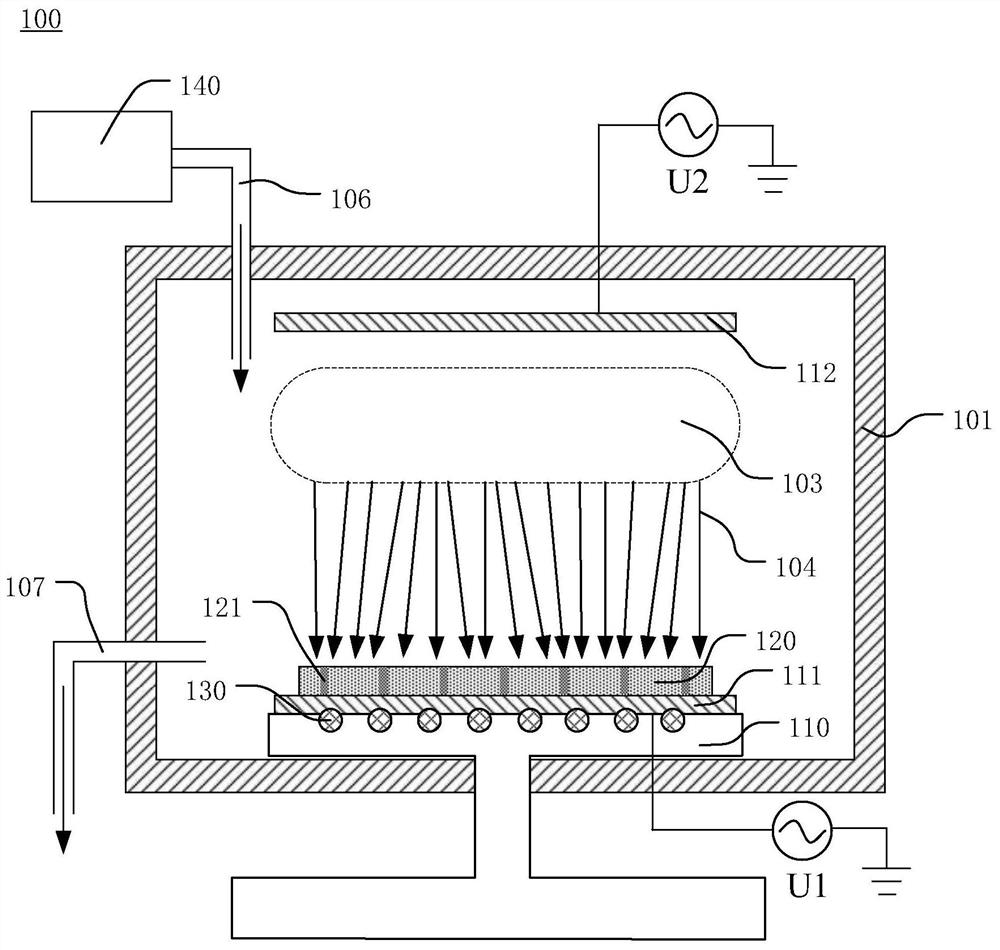
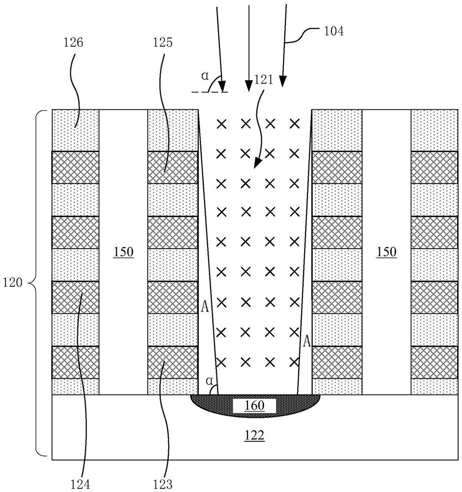
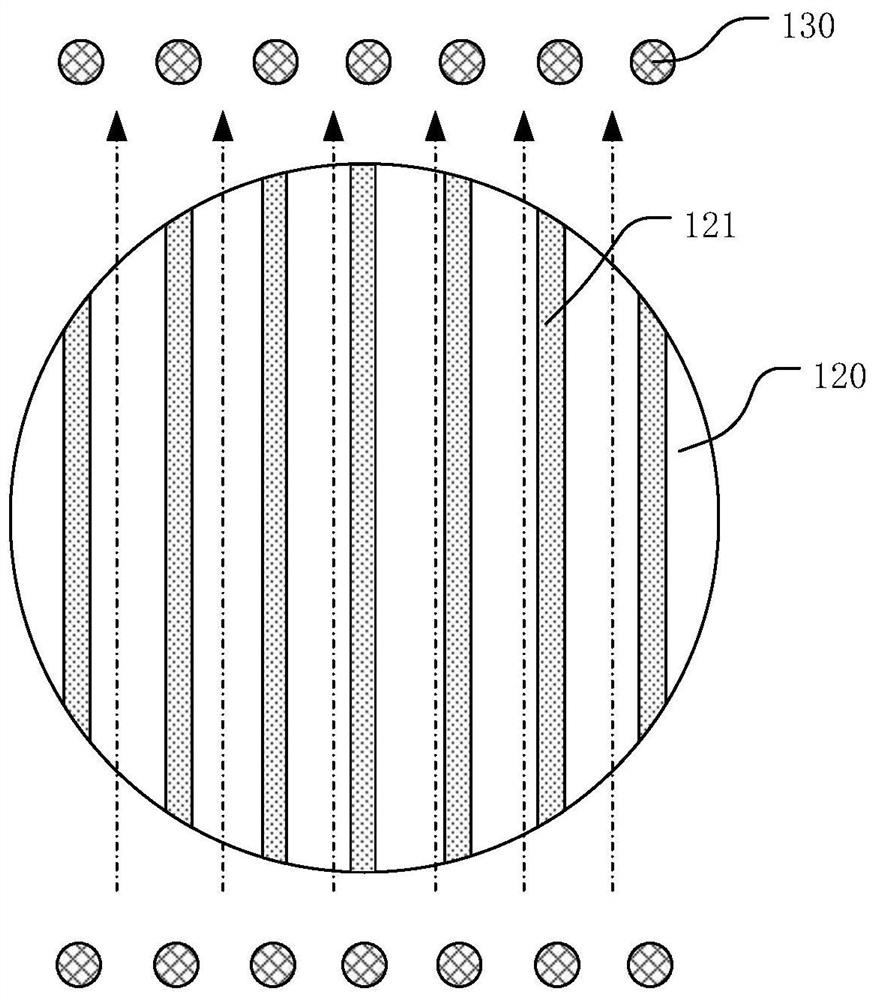
[0041] Hereinafter, the present invention will be described in more detail with reference to the accompanying drawings. In the various figures, identical elements are indicated with similar reference numerals. For the sake of clarity, various parts in the drawings have not been drawn to scale. Also, some well-known parts may not be shown. For the sake of simplicity, the semiconductor structure obtained after several steps can be described in one figure.

[0042] In the present application, the term "semiconductor structure" refers to a general designation of the entire semiconductor structure formed in various steps of manufacturing a memory device, including all layers or regions that have been formed. In the following, many specific details of the present invention are described, such as device structures, materials, dimensions, processing techniques and techniques, for a clearer understanding of the present invention. However, the invention may be practiced without these...


PUM


Abstract

The application discloses an ion implantation device and an ion implantation method. The ion implantation device includes: a reaction chamber; a gas supply source, connected to the reaction chamber, and injecting gas to be ionized into the reaction chamber; a carrying platform, located at the bottom of the reaction chamber, for carrying a wafer; The first electrode is located on the carrying platform, connected to the first power supply, and the wafer is located on the first electrode; the second electrode is located above the wafer, connected to the second power supply, and between the first electrode Generating an ion beam; a magnetic field generator, located on the first electrode or the carrying platform, for generating a magnetic field around the wafer, and changing the ion beam irradiation by adjusting the magnitude of the magnetic field generated by the magnetic field generator angle on the wafer. Therefore, when performing ion implantation on a wafer with a channel hole, the ion beam can be directly implanted into the bottom along an oblique angle without damaging the side wall.

Description

technical field [0001] The present invention relates to memory technology, and more specifically, to an ion implantation device and an ion implantation method. Background technique [0002] As the feature size of the semiconductor manufacturing process becomes smaller and smaller, the storage density of the memory device becomes higher and higher. At present, a storage device with a three-dimensional structure, that is, a 3D storage device, has been developed, which includes a plurality of storage units stacked in a vertical direction, and the integration level can be doubled on a wafer per unit area. Existing 3D memory devices, such as NAND memory devices, have fast writing speed and simple erasing operation, therefore, 3D memory devices adopting NAND structure have been widely used. Correspondingly, the manufacturing process of the NAND 3D storage device is constantly expanding, and commonly used processes include, for example, an etching process, a deposition process, an...

Claims


Application Information

Patent Timeline
Patent Type & Authority Patents(China)
IPC IPC(8): H01J37/317H01J37/32H01L21/265
CPCH01J37/317H01J37/32431H01J37/3266H01L21/26586
Inventor 刘小辉於成星张和周静兰刘修忠沈保家李军辉
Owner YANGTZE MEMORY TECH CO LTD
Why Eureka
Try Eureka