Display substrate, preparation method thereof and display device

A technology for display substrates and substrates, which is used in semiconductor/solid-state device manufacturing, semiconductor devices, electrical components, etc., and can solve problems such as transistor performance deterioration.

Pending Publication Date: 2021-05-28
BOE TECH GRP CO LTD
View PDF0 Cites 0 Cited by
  • Summary
  • Abstract
  • Description
  • Claims
  • Application Information

AI Technical Summary

Problems solved by technology

[0005] The technical problem to be solved by the present disclosure is to provide a display substrate and its preparati...

Method used


Image

  • Display substrate, preparation method thereof and display device
  • Display substrate, preparation method thereof and display device
  • Display substrate, preparation method thereof and display device

Examples


Embodiment Construction

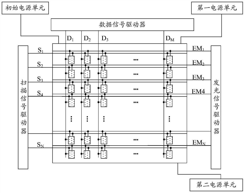
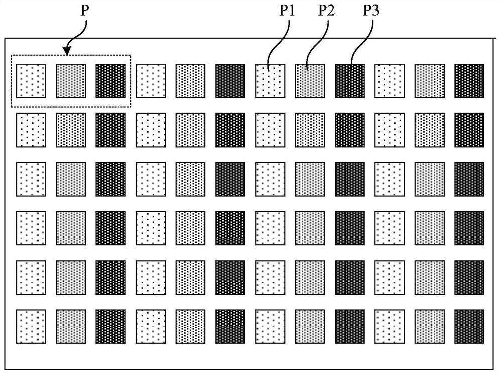
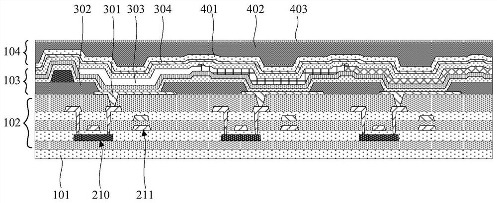
[0071] In order to make the purpose, technical solution and advantages of the present disclosure clearer, the embodiments of the present disclosure will be described in detail below in conjunction with the accompanying drawings. Note that an embodiment may be embodied in many different forms. Those skilled in the art can easily understand the fact that the means and contents can be changed into various forms without departing from the gist and scope of the present disclosure. Therefore, the present disclosure should not be interpreted as being limited only to the contents described in the following embodiments. In the case of no conflict, the embodiments in the present disclosure and the features in the embodiments can be combined arbitrarily with each other.

[0072] In the drawings, the size of each component, the thickness of a layer, or a region is sometimes exaggerated for the sake of clarity. Therefore, one aspect of the present disclosure is not necessarily limited to...


PUM


Abstract

The invention provides a display substrate, a preparation method thereof and a display device. The display substrate comprises a substrate body, an active structure layer arranged on the substrate body, a first source-drain structure layer arranged on the side, away from the substrate body, of the active structure layer, and a second source-drain structure layer arranged on the side, away from the substrate body, of the first source-drain structure layer. The active structure layer comprises a first active layer and a second active layer, the first source-drain structure layer comprises a first active via hole and a first source-drain electrode, and the first source-drain electrode is connected with the first active layer through the first active via hole; and the second source-drain structure layer comprises a second active via hole and a second source-drain electrode, and the second source-drain electrode is connected with the second active layer through the second active via hole. According to the invention, the uniformity of threshold voltage and starting current of the low-temperature polycrystalline silicon thin film transistor and the oxide thin film transistor is ensured, and the yield is improved.

Description

technical field [0001] The present disclosure relates to but is not limited to the field of display technology, especially to a display substrate, a manufacturing method thereof, and a display device. Background technique [0002] Organic Light Emitting Diode (OLED) is an active light-emitting display device, which has the advantages of self-illumination, wide viewing angle, high contrast, low power consumption, high response speed, light and thin, bendable and low cost. With the continuous development of display technology, a flexible display device (Flexible Display) which uses OLED as a light-emitting device and is signal-controlled by a Thin Film Transistor (TFT) has become a mainstream product in the display field. [0003] The inventors of the present application have found through research that existing OLED display substrates have the problem of poor transistor performance, which directly affects the display effect of OLED display devices. Contents of the invention...

Claims


Application Information

Patent Timeline
IPC IPC(8): H01L27/12H01L27/32H01L29/08H01L21/77
CPCH01L27/124H01L27/127H01L27/1229H01L29/0847H10K59/1213H10K59/131H01L27/1225H01L27/1248H10K59/122H10K59/126H10K59/1201H01L29/78672H01L29/7869H10K71/00
Inventor 刘文渠姚琪孟德天张锋崔钊董立文宋晓欣侯东飞王利波吕志军
Owner BOE TECH GRP CO LTD
Why Eureka
Try Eureka