A method for in-situ growth of refractory superstrong metal single crystal nanowires
An in-situ growth, single crystal nanotechnology, applied in the direction of single crystal growth, single crystal growth, crystal growth, etc.
- Summary
- Abstract
- Description
- Claims
- Application Information
AI Technical Summary
Problems solved by technology
Method used
Image
Examples
Embodiment
[0025] Concrete steps of the present invention are:
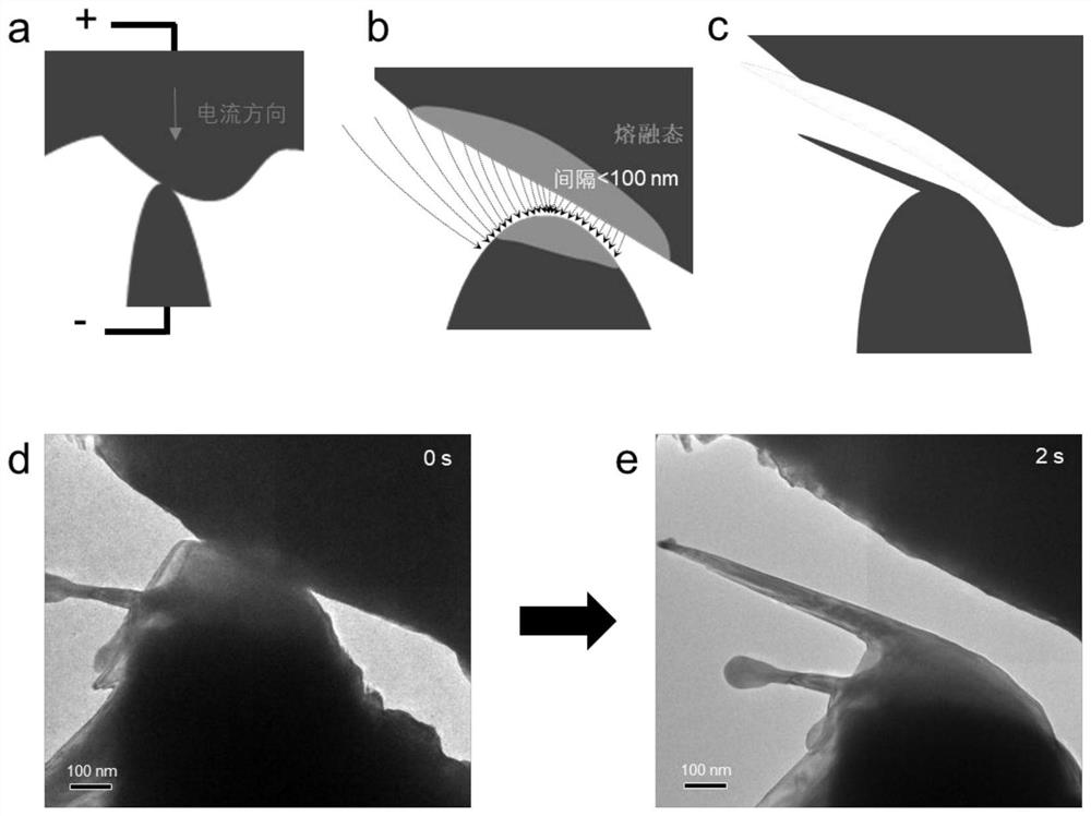
[0026] (1) Install the fracture surface of tungsten metal wire (0.25mm, purity 99.9wt.%) and electrochemically etched tungsten tip respectively on both ends of the in-situ electrical sample rod (Nanofactory STM-TEM holder) and put them into the electron microscope ( Titan 80-300), the radius of curvature of the needle tip is 3×10 -7 m, the radius of curvature of the protruding surface of the sample end is 8×10 -7 m, through the piezoelectric controller (Mains220V), the tip of the needle tip is in contact with the protruding surface of the sample end, and a constant voltage (8V) is applied to generate a current for Joule heating;
[0027] (2) By moving the tungsten tip to reduce the contact area of the two tips, as the contact area decreases, the current density of the contact point increases to melt and disconnect; the electric field enhanced by the curvature of the molten metal between the two disconnected tungsten tips ...
PUM
| Property | Measurement | Unit |
|---|---|---|
| aspect ratio | aaaaa | aaaaa |
| bending strength | aaaaa | aaaaa |
| diameter | aaaaa | aaaaa |
Abstract
Description
Claims
Application Information
 - R&D
- Intellectual Property
- Life Sciences
- Materials
- Tech Scout
- Unparalleled Data Quality
- Higher Quality Content
- 60% Fewer Hallucinations
Browse by: Latest US Patents, China's latest patents, Technical Efficacy Thesaurus, Application Domain, Technology Topic, Popular Technical Reports.
© 2025 PatSnap. All rights reserved.Legal|Privacy policy|Modern Slavery Act Transparency Statement|Sitemap|About US| Contact US: help@patsnap.com


