
Preparation method of high-thermal-conductivity net-size silicon nitride ceramic substrate

A technology of silicon nitride ceramics and net size, which is applied in the field of preparation of high thermal conductivity and net size silicon nitride ceramic substrates, which can solve the problems of low flatness, uneven thickness, substrate foaming, etc., and achieve high thermal conductivity , The effect of simple preparation process

Active Publication Date: 2021-05-25
SHANGHAI INST OF CERAMIC CHEM & TECH CHINESE ACAD OF SCI
View PDF7 Cites 5 Cited by
  • Summary
  • Abstract
  • Description
  • Claims
  • Application Information

AI Technical Summary

Problems solved by technology

Among them, due to the non-uniformity of powder flow and the process characteristics of mechanical pressing, the substrates formed by dry pressing often have difficulties such as direct preparation of ceramic substrates with a thickness of less than 0.5mm, the thickness cannot be accurately controlled, and the thickness is uneven. Hence the need for subsequent machining
The rolling film forming process is complicated, and it is necessary to repeatedly roll the film to eliminate the uneven thickness caused by the limitations of the process itself and the bumps caused by the agglomeration of raw materials, resulting in the prepared substrates prone to blistering and uneven surfaces. Machining can meet the subsequent copper clad process requirements
In contrast, the tape casting process has high production efficiency, low cost, can realize full automation, and is convenient for continuous batch production. It is the most promising and potential technology for ceramic substrate forming, but there are also tape casting The film is prone to blistering, cracking, deformation, uneven thickness, etc., resulting in problems such as low yield, low flatness, uneven thickness, and the need for subsequent machining

Method used

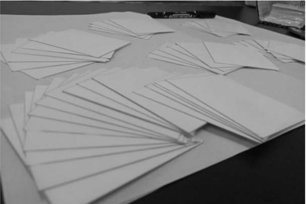
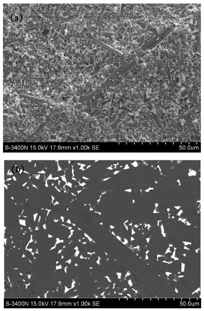
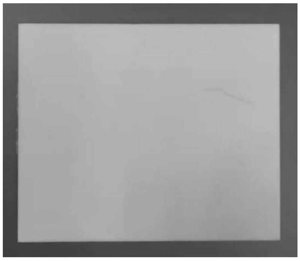

Image

  • Preparation method of high-thermal-conductivity net-size silicon nitride ceramic substrate
  • Preparation method of high-thermal-conductivity net-size silicon nitride ceramic substrate
  • Preparation method of high-thermal-conductivity net-size silicon nitride ceramic substrate

Examples


preparation example Construction

[0036] Preparation of agglomerate-free and bubble-free slurries. At least one of silicon nitride powder and silicon powder, sintering aid, dispersant, defoamer, binder and plasticizer in a protective atmosphere (such as N 2 atmosphere, the pressure can be 0.1MPa) after ball milling and mixing, and then vacuum degassing to prepare a mixed slurry without agglomeration and bubbles. In the ball milling process, silicon nitride ceramic grinding balls are used. The sintering aids can be rare earth oxides and alkaline earth metal oxides. The rare earth oxide contains at least Y 2 o 3 , the alkaline earth metal oxide contains at least MgO. The molar ratio between the rare earth oxide and the alkaline earth metal oxide may be (1.0-1.4): (2.5-2.9). Wherein when silicon powder is contained, the silicon powder content may be 75-100 wt%. Vacuumize the prepared slurry to remove air bubbles, the vacuum degree can be -0.1~-10kPa, and the degassing time can be 6~24h.

[0037] Preparatio...

Embodiment 1

[0045] First, the starting ceramic powder (silicon nitride 95g), sintering aid (5g, Y 2 o 3 : MgO=1.2:2.5, molar ratio), defoamer (oleic acid, 0.5g), dispersant (PEG, 0.5g), grinding ball (silicon nitride ball, 200g), organic solvent (absolute ethanol, 80g ) into a sealed nylon ball mill jar, and N 2 Atmosphere protection, ball mill mixing 4h under 100rpm; Further add binding agent (PVB, 7g) and plasticizer (DBP, 4g) in above-mentioned slurry, continue under N 2 After ball milling for 8 hours under the protection of the atmosphere, a uniformly dispersed and non-agglomerated slurry was obtained;

[0046] Secondly, vacuumize the prepared slurry to remove air bubbles for 12 hours, and the vacuum degree is -0.5kPa;

[0047] Subsequently, at N 2 Under a protective atmosphere, use a cylindrical scraper to tape-cast the above-mentioned slurry after removing air bubbles, and control the height of the scraper so that the thickness of the casting film blank is accurately controlled ...

Embodiment 2-5

[0054] Raw material ratio and composition, technical process refer to Example 1, specific parameters such as slurry preparation, vacuum degassing, tape casting, biscuit shaping, debonding and sintering process are as shown in Table 1, and the characteristics of the prepared substrate material are as follows Table 2 shows.


PUM

PropertyMeasurementUnit
Surface roughnessaaaaaaaaaa
Thermal conductivityaaaaaaaaaa
Flatnessaaaaaaaaaa

Abstract

The invention relates to a preparation method of a high-thermal-conductivity net-size silicon nitride ceramic substrate, which comprises the following steps of (1) mixing at least one of silicon nitride powder and silicon powder as original powder, a sintering aid, a dispersing agent, a defoaming agent, a binder and a plasticizer in a protective atmosphere, and performing vacuum degassing to obtain mixed slurry, (2) carrying out tape casting and drying in a nitrogen atmosphere to obtain a first biscuit, (3) carrying out shaping pretreatment on the obtained first biscuit to obtain a second biscuit, (4) debonding the obtained second biscuit in a nitrogen atmosphere with micro-positive pressure at 500-900 DEG C to obtain a third biscuit, and (5) placing the obtained third biscuit in a nitrogen atmosphere, and carrying out air pressure sintering at 1800-2000 DEG C to obtain the high-thermal-conductivity net-size silicon nitride ceramic substrate.

Description

technical field [0001] The invention relates to a method for preparing a silicon nitride ceramic substrate with high thermal conductivity and net size, and belongs to the field of ceramic material preparation. Background technique [0002] In recent years, semiconductor devices have developed rapidly along the direction of high power, high frequency, and integration. The heat generated by the operation of semiconductor devices is the key factor causing the failure of semiconductor devices, and the thermal conductivity of the insulating substrate is the key to affecting the overall heat dissipation of semiconductor devices. In addition, such as in the fields of electric vehicles and high-speed rail, semiconductor devices often face complex mechanical environments such as bumps and vibrations during use, which imposes strict requirements on the mechanical reliability of the materials used. [0003] High thermal conductivity silicon nitride (Si 3 N 4 ) Ceramics have excellen...

Claims


Application Information

Patent Timeline
IPC IPC(8): C04B35/593C04B35/622
CPCC04B35/5935C04B35/622C04B2235/3206C04B2235/3225C04B2235/6025C04B2235/606C04B2235/612C04B2235/656C04B2235/6567C04B2235/658C09K5/14C04B35/63488C04B2235/6582C04B2235/96C04B2235/963C04B2235/9638C04B2235/9607C04B35/632C04B2235/95C04B35/587C04B35/591C04B35/62218C04B35/6261C04B35/6264C04B35/62655C04B35/6303C04B35/6342C04B35/638C04B35/64C04B2235/3873C04B2235/428C04B2235/604C04B2235/6581C04B2235/6584C04B2235/661
Inventor 张辉刘学建蒋金弟姚秀敏黄政仁陈忠明
Owner SHANGHAI INST OF CERAMIC CHEM & TECH CHINESE ACAD OF SCI
Learn More