
Light-emitting diode display and manufacturing method thereof

A technology of light-emitting diodes and manufacturing methods, which is applied in the direction of semiconductor devices, static indicators, electric solid devices, etc., can solve problems such as increasing the complexity of circuit design and affecting the area utilization rate of high-resolution display screens, and achieve the reduction of circuit Complexity, increase transfer success rate, and reduce the effect of transfer times

Active Publication Date: 2021-04-16
INTERFACE TECH CHENGDU CO LTD +2
View PDF18 Cites 0 Cited by
  • Summary
  • Abstract
  • Description
  • Claims
  • Application Information

AI Technical Summary

Problems solved by technology

Reserved repair positions on the driver backplane can solve the problem of repairing bad pixels in mass transfer, but it will increase the complexity of circuit design, and also directly affect the future area utilization of high-resolution display screens

Method used


Image

  • Light-emitting diode display and manufacturing method thereof
  • Light-emitting diode display and manufacturing method thereof
  • Light-emitting diode display and manufacturing method thereof

Examples


Embodiment Construction

[0143] Embodiments of the present invention will be further explained with the help of related figures below. Wherever possible, the same reference numerals have been used throughout the drawings and description to refer to the same or similar components. In the drawings, the shape and thickness may be exaggerated for the sake of simplification and convenient labeling. It should be understood that elements not particularly shown in the drawings or described in the specification are forms known to those skilled in the art. Those skilled in the art can make various changes and modifications according to the content of the present invention.

[0144] When an element is referred to as being "on", it can generally mean that the element is directly on other elements, or there may be other elements present in between. Conversely, when an element is referred to as being "directly on" another element, it cannot have the other element in between. As used herein, the word "and / or" inc...


PUM

PropertyMeasurementUnit
sizeaaaaaaaaaa

Abstract

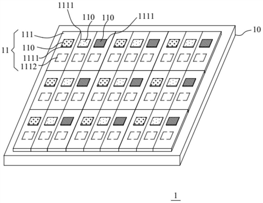
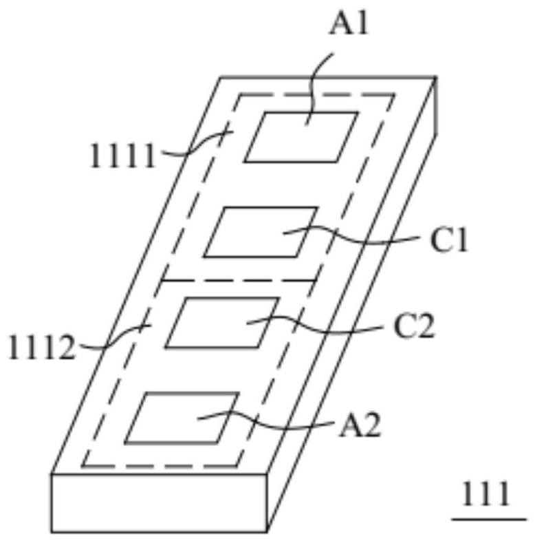
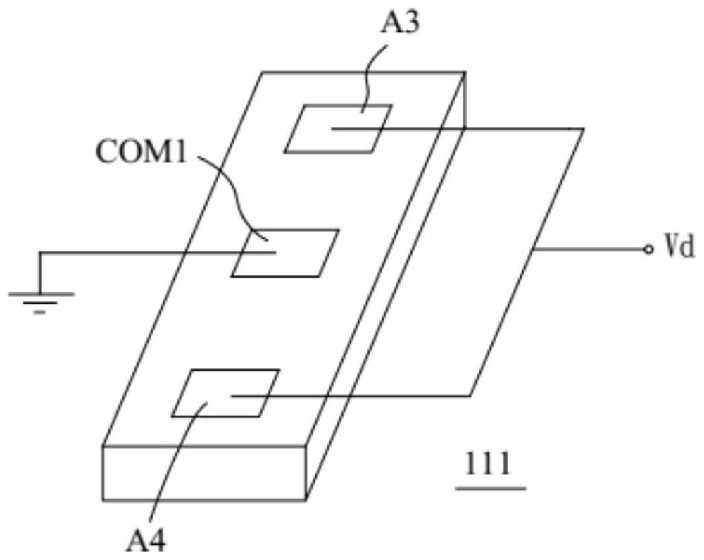
The invention discloses a light-emitting diode display and a manufacturing method thereof. The light-emitting diode display comprises a driving backboard and a plurality of pixel units; each pixel unit comprises at least one light-emitting diode and at least one packaging substrate; the top surface of each packaging substrate is provided with at least one conductive position and at least one conductive vacancy corresponding to the conductive position, wherein the conductive position is provided with a light-emitting diode, and the conductive position is electrically connected with the light-emitting diode on the conductive position; the bottom surface of the packaging substrate of each pixel unit is arranged on the driving backboard; and the driving backboard is electrically connected with the light-emitting diode of each pixel unit on the driving backboard and the conductive vacancy corresponding to the light-emitting diode. According to the light-emitting diode display and the manufacturing method thereof of the invention, the packaging substrates are arranged between the light-emitting diodes and the driving backboard, so that the complexity of a circuit for driving the backboard is reduced.

Description

technical field [0001] The invention relates to a manufacturing technology of a display, in particular to a light-emitting diode display and a manufacturing method thereof. Background technique [0002] Light-emitting diodes are regarded as a new generation of display technology, the overlord of the next generation of display technology. A large number of manufacturers at home and abroad are attacking one after another, and its market prospects are very promising. Light emitting diodes have a micron-level pitch, high brightness, low power consumption, ultra-high resolution and color saturation. The biggest advantage of light-emitting diodes comes from its biggest feature, each pixel can be addressed and controlled and single-point driven to emit light. [0003] In the manufacturing process, mass transfer is the most critical. Mass transfer is not to transfer one micro-light emitting diode at a time, but to transfer a lot of micro-light-emitting diodes from a growth substra...

Claims


Application Information

Patent Timeline
Patent Type & Authority Applications(China)
IPC IPC(8): G09F9/33G09G3/32H01L27/15H01L33/48H01L33/62
CPCG09G3/32H01L25/0753H01L33/0095H01L33/62H01L2933/0066H01L25/167G09G2320/045H01L22/20H01L22/22
Inventor 周贤颖陈伯纶陈俊达林柏青
Owner INTERFACE TECH CHENGDU CO LTD
Learn More