
IC die to IC die interconnection using error correcting code and data path interleaving

A technology for encoding data and decoding data, which is applied in electrical digital data processing, transmission link error control systems, circuits, etc., and can solve problems such as high silicon area cost, extra energy consumption, and increased heat generation

Pending Publication Date: 2021-04-13
HUAWEI TECH CO LTD
View PDF0 Cites 0 Cited by
  • Summary
  • Abstract
  • Description
  • Claims
  • Application Information

AI Technical Summary

Problems solved by technology

However, as bond pads are doubled for redundancy, the silicon area of ​​the bond pad array increases proportionally to redundancy, resulting in high silicon area cost, additional power dissipation from high capacitive loads, and resulting in heat generation increase

Method used


Image

  • IC die to IC die interconnection using error correcting code and data path interleaving
  • IC die to IC die interconnection using error correcting code and data path interleaving
  • IC die to IC die interconnection using error correcting code and data path interleaving

Examples


Embodiment Construction

[0032] It should be understood at the outset that, although an illustrative implementation of one or more embodiments is provided below, the disclosed systems and / or methods may be implemented using any number of techniques, whether currently known or in existence. The invention should in no way be limited to the illustrative implementations, drawings, and techniques illustrated below, including the exemplary designs and implementations illustrated and described herein, but rather be within the scope of the appended claims and their equivalents Modified within the full range of .

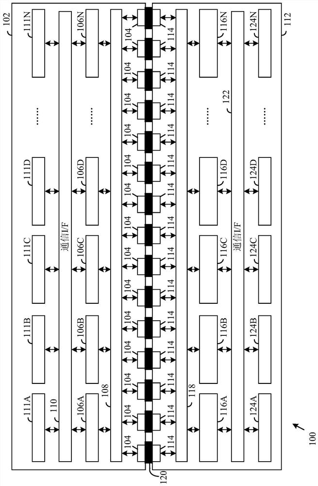
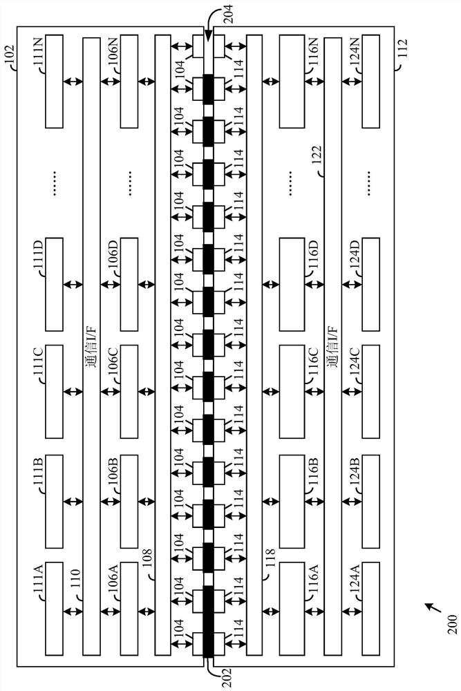
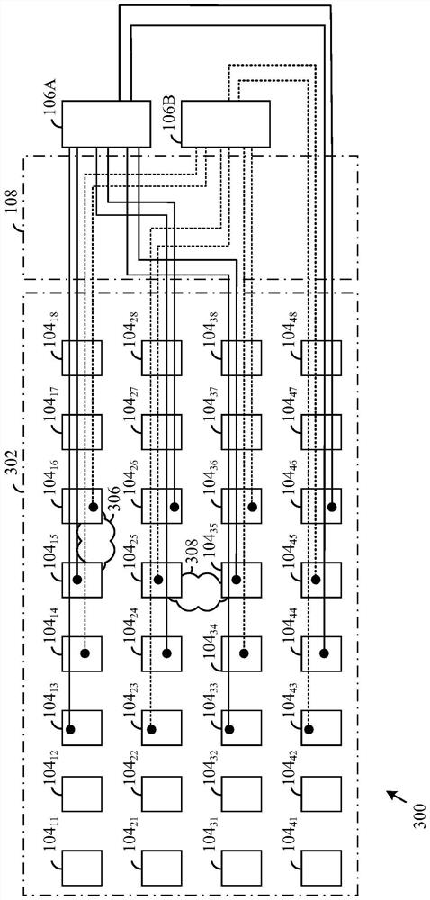
[0033] figure 1 is a cross-sectional side view illustrating a portion of a multi-chip module having a first integrated circuit (IC) die 102 and a second IC die 112 constructed in accordance with the described embodiments. The first IC die 102 includes a plurality of processing systems 111A- 111N coupled to each other through a communication interface 110 . Communication I / F 110 may be a NoC (or pa...


PUM


Abstract

A multi-chip module includes a first integrated circuit (IC) die a second IC die. The first IC die includes an array of first bond pads, a plurality of first code group circuits, and first interleaved interconnections between the plurality of first code group circuits and the array of first bond pads, and the first interleaved interconnections include a first interleaving pattern causing data from different code group circuits to be coupled to adjacent first bond pads. The second IC die includes a second array of bond pads that electrically couple to the array of first bond pads, a plurality of second code group circuits, and second interleaved interconnections between the plurality of second code group circuits and the array of second bond pads, and the second interleaved interconnections include a second interleaving pattern causing data from different code groups to be coupled to adjacent second bond pads.

Description

[0001] Related Applications Cross Application [0002] The title of the invention submitted by this application on September 12, 2018 is "IC Die To IC Die Interconnect Using Error Correcting Code And Data Path Interleaving" Priority to U.S. Provisional Patent Application Serial No. 62 / 730,048, which is hereby incorporated by reference as if reproduced herein in its entirety. technical field [0003] The present application relates to integrated circuit (IC) technology, and more particularly to communication between IC dies of a multi-chip module. Background technique [0004] Integrated circuit (IC) technology has made great progress over the past fifty years. ICs are now ubiquitous and found in electronic equipment, machines, vehicles, appliances and many other devices. Large processing ICs now include billions of transistors, while memory ICs include hundreds of billions of transistors. The density of transistors on an IC can reach 100 million transistors per square mil...

Claims


Application Information

Patent Timeline
IPC IPC(8): H01L23/525
CPCH01L2224/131H01L2224/16145H01L2224/0401H01L2224/05647H01L2224/08145H01L2224/06181H01L2224/02375H01L2224/02373H01L2224/06131H01L24/06H01L24/08H01L24/13H01L24/16H01L25/04H01L25/18G06F13/4265H04L2001/0094H04L2001/0096H04L1/0041H01L2924/014H01L2924/00014G06F13/4027H01L22/34H01L25/0657H01L2225/06596
Inventor 顾识群
Owner HUAWEI TECH CO LTD
Learn More