
Preparation method of high-performance DFB laser epitaxial wafer

An epitaxial wafer, high-performance technology, applied in the field of optical communication, can solve the problems of poor etching uniformity, low product yield, affecting the secondary epitaxial growth of products, etc., to achieve the effect of improving uniformity and reducing costs

Pending Publication Date: 2021-04-09
全磊光电股份有限公司
View PDF5 Cites 1 Cited by
  • Summary
  • Abstract
  • Description
  • Claims
  • Application Information

AI Technical Summary

Problems solved by technology

However, traditional etching methods have disadvantages. Bromic acid solution is used for wet etching, but the solution has no selectivity for InP / InGaAsP, the grating depth is difficult to control, the etching uniformity is poor, and the product yield is extremely low.
Invention patent 201310008696.8 uses an etching solution composed of HCL, H3PO4 and H2O to etch away a layer of InP layer, then uses an etching solution composed of H2SO4, H2O2 and water to etch away InGaAsP, and finally removes the photoresist to obtain a laser grating; but HCL The etching solution composed of , H3PO4 and H2O can only etch InP, which has obvious anisotropy. After etching, InP presents an inverted trapezoid, which affects the secondary epitaxial growth of the product.

Method used


Image

  • Preparation method of high-performance DFB laser epitaxial wafer
  • Preparation method of high-performance DFB laser epitaxial wafer
  • Preparation method of high-performance DFB laser epitaxial wafer

Examples


preparation example Construction

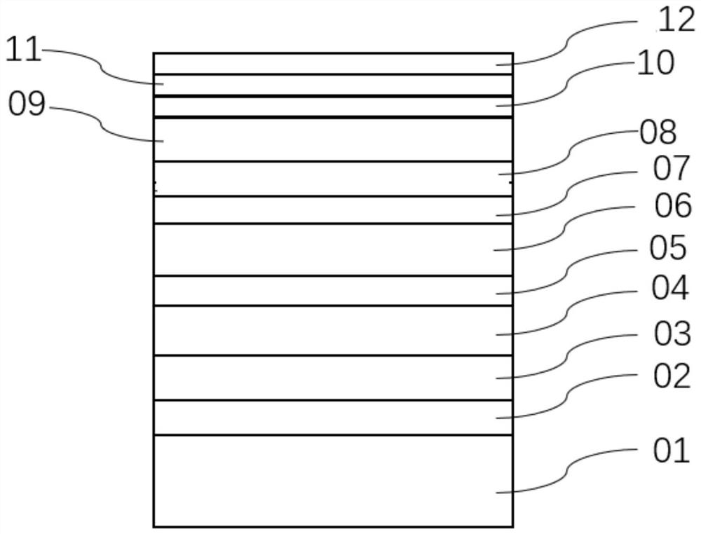
[0026] This patent discloses a method for preparing a high-performance DFB laser epitaxial wafer, which specifically includes the following steps:

[0027] First as figure 1 As shown, put the InP substrate 01 into the MOCVD equipment, and deposit growth buffer, 02, confinement layer 03, lower waveguide layer 04, quantum well layer 05, upper waveguide layer 06, The upper confinement layer 07, the buffer layer 08, the etching barrier layer 09, the InP cladding layer 10, the grating layer 11, and the InP cap layer 12 form a primary epitaxial wafer structure, wherein the grating layer 11 is an InGaAsP grating layer.

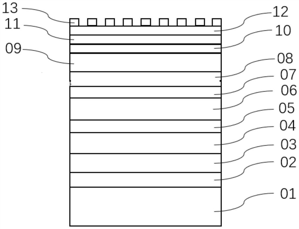
[0028] like figure 2 As shown, the epitaxial wafer is taken out from the MOCVD equipment, photoresist is spin-coated on the InP cap layer 12 of the epitaxial wafer, and a photoresist mask 13 is formed by holographic lithography.

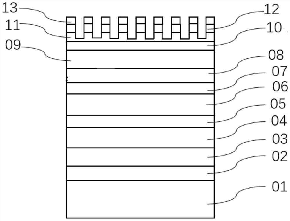
[0029] like image 3 As shown, the epitaxial wafer is etched with an etching solution, and the InP cap layer 12 and part of the InGaAs...


PUM

PropertyMeasurementUnit
thicknessaaaaaaaaaa
thicknessaaaaaaaaaa

Abstract

The invention discloses a preparation method of a high-performance DFB laser epitaxial wafer, and the method comprises the following steps of: firstly, sequentially depositing and growing a buffer layer, a limiting layer, a lower waveguide layer, a quantum well layer, an upper waveguide layer, an upper limiting layer, a buffer layer, a corrosion barrier layer, an InP cladding, a grating layer and an InP cap layer on an InP substrate from bottom to top, then performing photoresist homogenizing, exposure and development, and etching the epitaxial wafer with an etching solution twice, etching a grating layer for the first time and reserving the grating layer with a certain thickness, then removing the photoresist, etching the remaining grating layer with a selective etching solution for the second time, and finally carrying out secondary growth on the epitaxial wafer, wherein an InP layer, a barrier gradient layer and an ohmic contact layer sequentially grow from bottom to top. Two etching solutions are adopted for grating etching, a photoresist mask on the surface is removed by etching to the position of the grating layer for the first time, and a solution with selective corrosion is used for etching the remaining grating layer for the second time, so that the uniformity of grating etching and the uniformity of grating duty are improved, and the performance of the DFB laser is improved.

Description

technical field [0001] The invention relates to the field of optical communication, in particular to a preparation method of a high-performance DFB laser epitaxial wafer used in the field of optical communication. Background technique [0002] Optical communication networks use light as the carrier of signal transmission. Compared with electrical communication networks that use copper cables as transmission media, the speed, capacity and anti-interference ability of information interconnection are significantly improved, so they are widely used. Semiconductor lasers are the main light sources for optical communication networks, including three types of Fabry-Perot lasers (FP lasers), distributed feedback lasers (DFB) and vertical cavity surface emitting lasers (VCSELs). Among them, the DFB laser establishes a Bragg grating inside the semiconductor, and relies on the distributed feedback of light to realize the selection of single longitudinal mode, which has the characterist...

Claims


Application Information

Patent Timeline
Patent Type & Authority Applications(China)
IPC IPC(8): H01S5/12C09K13/04
CPCC09K13/04H01S5/12H01S2304/04
Inventor 李洪雨张永单智发姜伟陈阳华
Owner 全磊光电股份有限公司
Learn More