Manufacturing method of single-curved-surface silicon-based micro display

A technology of micro-display and manufacturing method, applied in semiconductor/solid-state device manufacturing, electric solid-state devices, semiconductor devices, etc., can solve problems such as poor sealing layer effect, achieve the effect of reducing weight and improving comfort

Inactive Publication Date: 2021-04-06
浙江宏禧科技有限公司
View PDF5 Cites 1 Cited by
  • Summary
  • Abstract
  • Description
  • Claims
  • Application Information

AI Technical Summary

Problems solved by technology

[0004] The technical problem to be solved by the present invention is to provide a method for manufacturing a single-curved silicon-based microdisplay, which can improve the shortcomings of the thinned wafer being fragile in the cutting process and the poor sealing layer effect after bending. Under the magnification, reduce the weight of the optical system and improve the comfort of wearable devices

Method used


Image

  • Manufacturing method of single-curved-surface silicon-based micro display
  • Manufacturing method of single-curved-surface silicon-based micro display
  • Manufacturing method of single-curved-surface silicon-based micro display

Examples


Embodiment 1

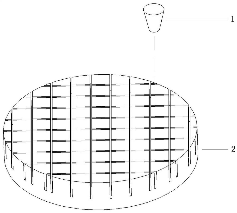
[0034] like Figures 1 to 3 Shown, a kind of manufacturing method of single-curved silicon-based microdisplay, comprises the following steps:

[0035] Step 1, UV laser cutting, using a 355 nm UV laser 1 on the front side of the wafer 2 with a thickness of 400 microns to perform vertical and horizontal laser scribing and cutting, wherein the focal spot of the UV laser 1 is 20 microns, and the depth of the cutting line is 100 microns, followed by Soak in acetone, ethanol, and deionized water for 10 minutes each to clean the wafer 2;

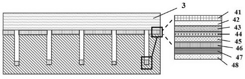
[0036] Step 2, preparing an OLED display 7, depositing patterned anode pixel points 48, a hole functional layer 47, an organic light-emitting layer 46, an electronic functional layer 45, a transparent cathode layer 44, a sealing layer 43, and a color filter layer sequentially on the wafer 2 42 and a physical protection layer 41, and a plurality of flat OLED displays 7 are prepared on the front surface of the wafer 2. The sealing layer 43 is a mul...

Embodiment 2

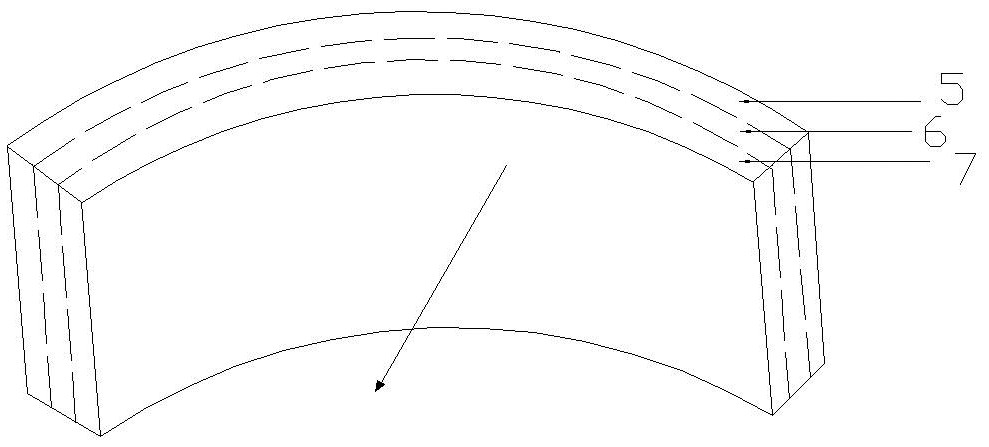
[0045] like Figure 4 As shown, in this embodiment, the curved surface of the curved micro-display is concave in the horizontal direction, the light source is emitted from the stainless steel bracket toward the display, and other structures are the same as in the first embodiment.

Embodiment 3

[0047] like Figure 5 As shown, in this embodiment, the curved surface of the curved microdisplay is convex in the vertical direction, and the light source is emitted from the stainless steel bracket toward the display, and other structures are the same as in Embodiment 1.


PUM

PropertyMeasurementUnit
Curved arcaaaaaaaaaa
Wavelengthaaaaaaaaaa
Thicknessaaaaaaaaaa

Abstract

The invention discloses a manufacturing method of a single-curved-surface silicon-based micro display, which comprises the steps of ultraviolet laser cutting, preparation of an OLED display, attachment of a front protective film, wafer thinning, separation of the display, adhesion of a flexible back plate, welding, curved surface fixing and the like, so as to form the silicon-based curved-surface micro display. According to the method, the characteristic that the silicon wafer is fragile in the cutting process after being thinned is avoided through the half-cutting technology, the buffer layer is added into the sealing layer, the interlayer bending stress is relieved, the weight of an optical system can be reduced through the curved-surface micro OLED displayer under the same magnification, and the comfort degree of the wearable device is improved.

Description

technical field [0001] The invention relates to the technical field of displays, in particular to a method for manufacturing a single-curved silicon-based microdisplay. Background technique [0002] The substrate materials of curved organic light-emitting diode (OLED) displays mainly include glass and silicon wafers. Curved displays based on transparent materials such as glass have the advantages of improving viewing angle range and overall aesthetics, and are often used in medium and large-sized display fields such as TVs, mobile phones, and computers. However, curved OLED displays based on silicon wafers have received more attention and research due to the advantages of ultra-high resolution, color purity, small size and easy portability that traditional OLED displays do not have. Silicon-based curved OLED displays can be used in Wearable devices, such as AR smart glasses, smart watches, etc. [0003] At this stage, silicon-based curved OLED microdisplays have not yet be...

Claims


Application Information

Patent Timeline
IPC IPC(8): H01L27/32H01L51/56
CPCH10K59/10H10K71/00
Inventor 吴康敬孙扬李德权颜艳霜杨震元
Owner 浙江宏禧科技有限公司
Why Eureka
Try Eureka