


Quick Research
Generate reliable direction feasibility study reports for your R&D in just a few steps.

Technical Q&A
Discover and master advanced knowledge NOW. Basics, ideas, possibilities, all at once.

Find Solutions
As an expert in R&D theories, this can generate solutions to your technical problems instantly.

Evaluate Feasibility
Analyze your overall solution with one click, know your potential R&D risks in advance.

Monitor Landscape
Get weekly tech updates, stay abreast of the latest tech innovations and key insights.
Software-on-chip defined interconnection network device and method
A software-defined and interconnected network technology, applied in static memory, instruments, etc., can solve problems such as insufficient support for wafer-level integration, and achieve the effects of reducing design costs, flexible connections, and improving testability
- Summary
- Abstract
- Description
- Claims
- Application Information
AI Technical Summary
Problems solved by technology
Method used
Image

Examples
Embodiment 1
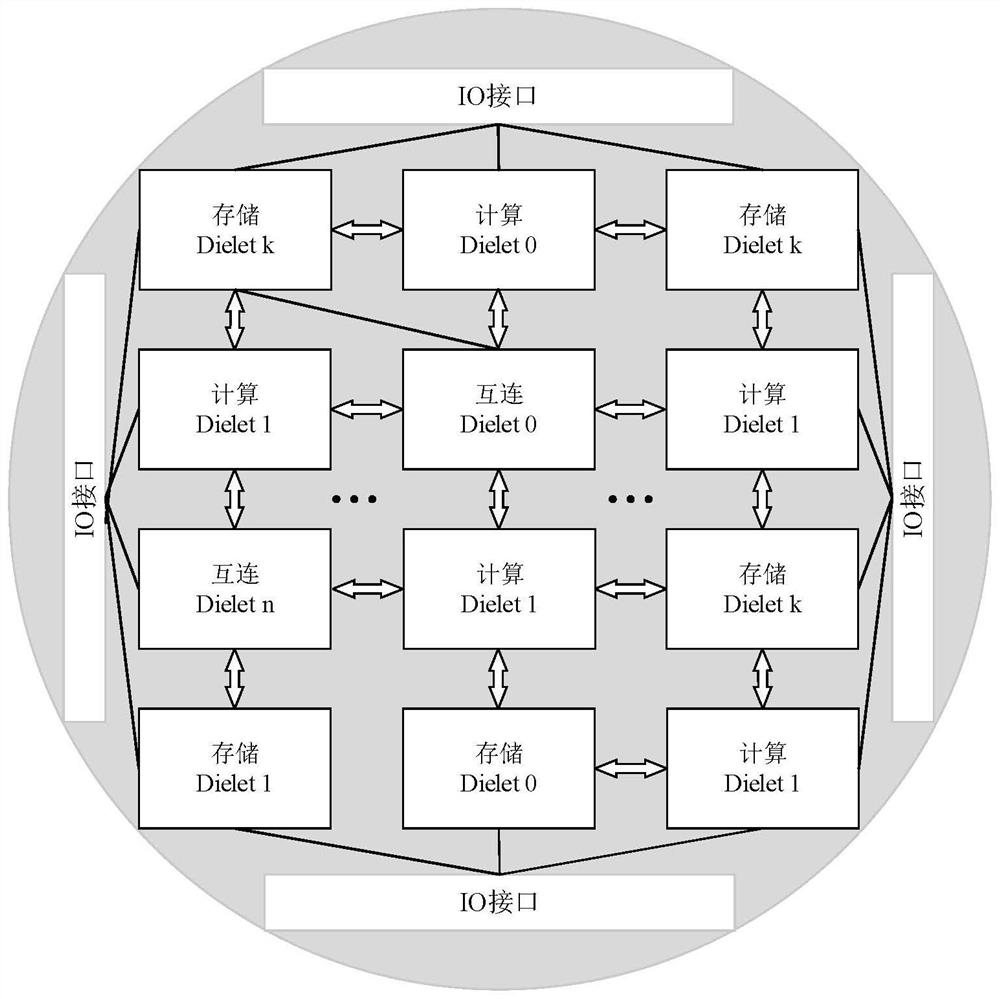
[0024] like figure 1 As shown, an embodiment of the present invention provides an on-chip software-defined interconnection network device, including: a silicon substrate and a system-on-chip network arranged on the silicon substrate, and nodes in the system-on-chip network include computing nodes and storage nodes and a network node, where the network node includes an on-chip routing device (Router On Wafer, RoW); wherein, each node in the system-on-chip system network is interconnected through the on-chip routing device.
[0025] Specifically, considering that computing resources, storage resources, and network resources are the three basic types of resources in hardware infrastructure, the system-on-chip network in this embodiment also includes the above three types of nodes during design. The interconnection lines of the on-chip routing device in this embodiment are physically fixed and immutable, and logically can be software-defined according to application requirements, ...
Embodiment 2
[0028] On the basis of the above-mentioned embodiments, this embodiment of the present invention also provides an on-chip software-defined interconnection network device, which is different from the above-mentioned embodiment 1 in that in this embodiment, the on-chip routing device includes a first An on-chip routing device and a second on-chip routing device; wherein, one port of the first on-chip routing device is used to connect to the second on-chip routing device, and the remaining ports are used to connect to the other ports of the on-chip system network. Nodes other than the second on-chip routing device; each port of the second on-chip routing device is used to connect to one of the first on-chip routing devices.
[0029] Specifically, the software-defined on-chip routing device is mainly used to connect computing nodes, storage nodes, and network nodes within the on-chip system network, and each on-chip routing device can connect up to N (N≥2) nodes. In practical appl...
Embodiment 3
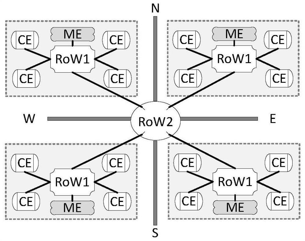
[0034] Corresponding to the above-mentioned on-chip software-defined interconnection network device, an embodiment of the present invention also provides an on-chip software-defined interconnection network method, including: dividing the nodes in the system-on-chip system network into clusters, and each cluster includes computing nodes , a storage node and an on-chip routing device; each node in the cluster is connected using a software-defined interconnection structure.
[0035]Specifically, the software-defined interconnect structure can refer to "Lu Ping, Liu Qinrang, Wu Jiangxing, etc. A new generation of software-defined architecture [J]. Chinese Science: Information Science, 2018 (3).", no more details here . By using a software-defined interconnection structure for connection, the interconnection between these nodes has the characteristics of high bandwidth, low latency, frequent communication, and various modes, and can be flexibly defined through software-defined inte...
PUM
| Property | Measurement | Unit |
|---|---|---|
| The maximum diameter | aaaaa | aaaaa |
Abstract
Description
Claims
Application Information
 - R&D Engineer
- R&D Manager
- IP Professional
- Industry Leading Data Capabilities
- Powerful AI technology
- Patent DNA Extraction
Browse by: Latest US Patents, China's latest patents, Technical Efficacy Thesaurus, Application Domain, Technology Topic, Popular Technical Reports.
© 2024 PatSnap. All rights reserved.Legal|Privacy policy|Modern Slavery Act Transparency Statement|Sitemap|About US| Contact US: help@patsnap.com