Method for manufacturing flow sensor chip

A technology of flow sensor and manufacturing method, which is applied in the direction of exposure device, coating, gaseous chemical plating, etc. of photolithography process, and can solve the problems of reducing the stability of the sensor, reducing the service life of the sensor, and being unable to accurately control the corrosion area and depth, etc. Achieve the effects of improving device stability, flat sensor surface, and realizing diversity

Active Publication Date: 2021-03-16
长芯科技(上海)有限公司
View PDF8 Cites 1 Cited by
  • Summary
  • Abstract
  • Description
  • Claims
  • Application Information

AI Technical Summary

Problems solved by technology

[0003] For example, a Chinese invention patent with the publication number CN102491260A discloses a method for manufacturing a flow sensor by corrosion self-stopping method and a Chinese invention patent with the publication number CN102515087A discloses a method for manufacturing a flow sensor, both through the back The cavity formed by the corrosion process is mainly through the precise control of time, which is closely related to the purity, concentration and temperature of the corrosion solution used. It is impossible to accurately control the corrosion area and depth. The back of the corrosion substrate is recessed inward to form a groove to realize the sensor If it is set in the air, the back corrosion will penetrate the entire substrate, which will reduce the stability of the overall structure of the sensor to a certain extent, and greatly reduce the life of the sensor.

Method used


Image

  • Method for manufacturing flow sensor chip
  • Method for manufacturing flow sensor chip
  • Method for manufacturing flow sensor chip

Examples


Embodiment Construction

[0047] The invention discloses a manufacturing method of a flow sensor chip, in particular to a manufacturing method that can not damage the stability and strength of the overall structural plate of the chip.

[0048] The present invention will be described in further detail below in conjunction with the accompanying drawings and an embodiment of the present invention.

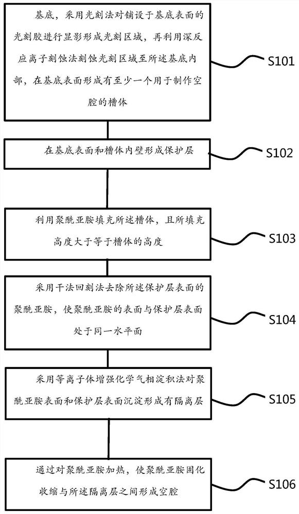
[0049] Such as figure 1 As shown, the method steps for manufacturing the flow sensor include:

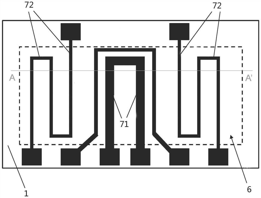
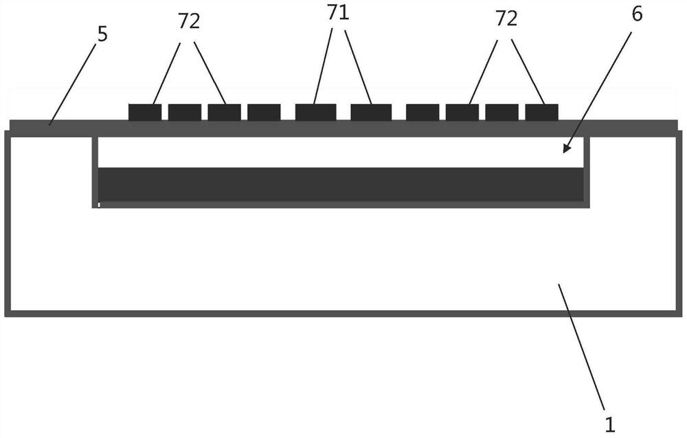
[0050] Step S101: substrate 1, using photolithography to develop the photoresist laid on the surface of substrate 1 to form a photoresist area, and then using deep reactive ion etching to etch the photoresist area to the inside of substrate 1 to form a photoresist on the surface of substrate 1 There is at least one tank body 2 for making a cavity 6;

[0051] Step S102: forming a protective layer 3 on the surface of the substrate 1 and the inner wall of the tank body 2;

[0052] Step S103: Fill the tank body 2 wit...


PUM

PropertyMeasurementUnit
thicknessaaaaaaaaaa

Abstract

The invention provides a method for manufacturing a flow sensor chip. The method comprises the following steps that regarding a base, photoresist paved on the surface of the base is developed througha photoetching method to form a photoetching region, the photoetching region is etched to reach the interior of the base through a deep reactive ion etching method, and at least one groove body for manufacturing a cavity is formed in the surface of the base; a protective layer is formed on the surface of the base and the inner wall of the groove body; the groove body is filled with polyimide, wherein a filling height is greater than or equal to a height of the groove body; the polyimide on the surface of the protective layer is removed through a dry back-etching method, so that the surface ofthe polyimide and the surface of the protective layer are positioned on the same horizontal plane; the polyimide surface and the protective layer surface are precipitated through a plasma enhanced chemical vapor deposition method to form an isolation layer; and the polyimide is heated, so that the polyimide is solidified and contracted to form a cavity with the isolation layer. The method has goodstructural stability and is suitable for mass production.

Description

technical field [0001] The invention relates to the technical field of semiconductor technology, in particular to a method for manufacturing a flow sensor chip. Background technique [0002] At present, flow sensors have been widely used in the detection of gas flow in automobile engines, oil and gas, and medical equipment. In the existing structure of some temperature-related semiconductor sensors, it is sometimes necessary to place the sensor on a suspended film. After packaging, the substrate under the sensor is not in contact with the base of the package, but is suspended and in contact with air or vacuum to achieve The purpose of reducing the external environment temperature interference. [0003] For example, a Chinese invention patent with the publication number CN102491260A discloses a method for manufacturing a flow sensor by corrosion self-stopping method and a Chinese invention patent with the publication number CN102515087A discloses a method for manufacturing a...

Claims


Application Information

Patent Timeline
Patent Type & Authority Applications(China)
IPC IPC(8): C23C16/50G03F7/20
CPCC23C16/50G03F7/20
Inventor 陈志宝
Owner 长芯科技(上海)有限公司
Why Eureka
Try Eureka