Method for selectively plating inner blind hole of ultrathin plate

A technology of plating and blind hole selection, applied in the field of PCB manufacturing, can solve the problems of enlarged blind hole sag value and board size deformation, and achieve the effect of reducing rework rate, ensuring product quality, and ensuring accurate alignment

Active Publication Date: 2021-03-12
惠州市大亚湾科翔科技电路板有限公司
View PDF3 Cites 0 Cited by
  • Summary
  • Abstract
  • Description
  • Claims
  • Application Information

AI Technical Summary

Problems solved by technology

[0007] The embodiment of the present application provides a method for selective plating of blind holes in the inner layer of ultra-thin boards, and by setting the blind hole selective plating process, the problems of board size deformation and blind hole depression value are solved, thereby ensuring product yield and reducing The risk of quality loss greatly reduces the rework rate, effectively improves the process capability, improves production efficiency, and improves the core competitiveness of the production process

Method used


Image

  • Method for selectively plating inner blind hole of ultrathin plate

Examples


Embodiment

[0026] In order to facilitate those skilled in the art to understand the present invention, the present invention will be further described in detail below in conjunction with specific embodiments and accompanying drawings.

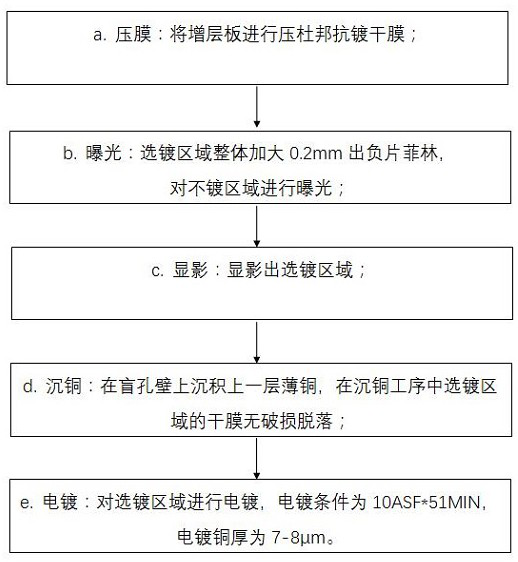
[0027] A method for selective plating of blind holes in the inner layer of an ultra-thin plate is completed according to the following steps:

[0028] a. Film pressing: press the build-up board with DuPont anti-plating dry film;

[0029] b. Exposure: The blind hole point and the area that accepts the blind hole point are used as the selective plating area, and the rest of the area is used as the non-plating area. The selective plating area is enlarged by 0.2mm as a whole, and the negative film is released, and it is placed under the irradiation of a purple light to undergo polymerization. Cross-linking reaction, exposure to unplated areas;

[0030] c. Developing: develop the selected plating area;

[0031] d. Copper sinking: use chemical methods to depo...


PUM


Abstract

The invention discloses a method for selectively plating an inner blind hole of an ultrathin plate. The method comprises the steps of pressing a film, specifically, pressing a Dupont anti-plating dryfilm on a laminated plate; conducting exposure, specifically, taking the blind hole point position and the area bearing the blind hole point position as a selective plating area, taking other areas asnon-plating areas, integrally enlarging the selective plating area by 0.2 mm to form a negative film, and exposing the non-plating areas; developing, specifically, developing the selective plating area; conducting copper deposition, specifically, depositing a layer of thin copper on the wall of the blind hole by using a chemical method, wherein a dry film in the selective plating area in the copper deposition process is not damaged and falls off; and conducting electroplating, specifically, conducting electroplating on the selective plating area, wherein the electroplating condition is 10ASF* 51 MIN, and the electroplating copper thickness is 7-8 microns. The problems of plate size deformation and blind hole sinking value increasing are solved by setting the blind hole selective platingprocess, so that the product yield is guaranteed, the quality loss risk is reduced, the rework rate is greatly reduced, the processing capacity is effectively improved, the production efficiency is improved, and the core competitiveness of the production process is improved.

Description

technical field [0001] The invention belongs to the technical field of PCB manufacturing, and in particular relates to a method for selective plating of blind holes in an inner layer of an ultra-thin board. Background technique [0002] In the existing technology, the general process design of the inner layer blind hole is laser drilling + immersion copper + hole filling electroplating. This kind of design is not suitable for stacked blind hole products with ultra-thin copper thickness, because the inner layer copper thickness is relatively thin According to the conventional process requirements, the board after hole filling and electroplating needs to be acid-etched to meet the copper thickness requirements. [0003] The production difficulties brought by conventional methods are: [0004] 1. The board that has been etched to reduce copper needs to be brushed to meet the roughness of the copper surface, but the thin board cannot be brushed and ground to easily cause dimens...

Claims


Application Information

Patent Timeline
Patent Type & Authority Applications(China)
IPC IPC(8): H05K3/42
CPCH05K3/424
Inventor 王康兵周刚唐文锋
Owner 惠州市大亚湾科翔科技电路板有限公司
Why Eureka
Try Eureka