A casting single crystal seed crystal laying method with short bottom red zone and few primary dislocations

A laying method and single crystal technology, applied in the direction of single crystal growth, single crystal growth, chemical instruments and methods, etc., can solve the problems of original dislocation, lower crystal quality, stress concentration, etc., to reduce distortion and reduce quantity , the effect of shortening the length

Active Publication Date: 2022-03-22
NANCHANG UNIV
View PDF5 Cites 0 Cited by
  • Summary
  • Abstract
  • Description
  • Claims
  • Application Information

AI Technical Summary

Problems solved by technology

Among them, the surface roughness of the cast single crystal seed crystal is small after cleaning, and the surface roughness of the silicon wafer is also small. The cast single crystal seed crystal is directly spread on the bottom of the crucible or on the silicon wafer at the bottom of the crucible. There are point or line contacts between the cast single crystal seeds, between the cast single crystal seeds and the silicon material, these positions will generate stress concentration, and it is easy to generate native dislocations
The diffusion speed of impurities on the free surface>grain boundary>inside the crystal, so a layer of silicon wafers or several layers of silicon wafers are laid on the bottom of the crucible (several layers of silicon wafers cannot be completely bonded), so that the impurities at the bottom of the crucible can easily diffuse to Cast single crystal seed crystals and inside cast single crystal silicon ingots, these impurities lead to the length of the red area at the bottom of the cast single crystal silicon ingots, and impurities can also easily cause lattice distortion of silicon crystals, thereby generating dislocation sources and reducing crystal quality

Method used


Image

  • A casting single crystal seed crystal laying method with short bottom red zone and few primary dislocations
  • A casting single crystal seed crystal laying method with short bottom red zone and few primary dislocations
  • A casting single crystal seed crystal laying method with short bottom red zone and few primary dislocations

Examples


Embodiment 1

[0046] Example 1: Production of cast single crystal silicon ingots by conventional casting single crystal seed laying method (comparative example)

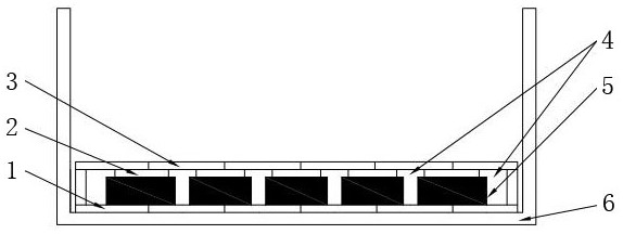
[0047] S11. Remove the head, tail and edge of the Czochralski monocrystalline silicon rod, and wire-cut it to obtain a cast single crystal seed crystal. The size of each cast single crystal seed crystal is 158mm×158mm×25mm. Wash the cast single crystal seed crystal with pure water first. Remove surface dirt, then clean with acid or lye to remove mechanical damage on the surface of the seed crystal, and finally wash away residual acid or lye with pure water;

[0048]S12. Pickling the scrapped silicon wafers, laying a layer of scrapped silicon wafers on the bottom of the crucible, the size of the silicon wafers is 158mm×158mm×0.18mm, and laying a layer of cast single crystal seed crystals on the silicon wafers;

[0049] S13. laying 25 pieces of cast single crystal seed crystals on the first thick layer, and closely bonding between a...

Embodiment 2

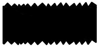
[0052] S21. Remove the head, tail and edge of the Czochralski monocrystalline silicon rod, and wire-cut it to obtain a cast single crystal seed crystal. The size of each cast single crystal seed crystal is 158mm×158mm×25mm. The upper and lower surfaces of the cast single crystal seed crystal are Sandblasting to increase its roughness, with a roughness value of 50 microns, such as figure 2 shown;

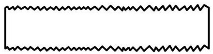
[0053] S22. Cut a slab from a polycrystalline silicon block or a monocrystalline silicon block, the slab size of the first slab layer and the third slab layer is 158mm×158mm×3mm, and the slab size of the second slab layer is 145mm× 145mm×3mm, sandblasting the upper and lower surfaces of the thick sheet to increase its roughness, the roughness value is 50 microns, such as image 3 shown;

[0054] S23. Laying 36 slabs on the bottom of the crucible, the sides of adjacent slabs are closely attached to form the first slab, the first slab covers the entire bottom of the crucible, and th...


PUM

PropertyMeasurementUnit
surface roughnessaaaaaaaaaa
thicknessaaaaaaaaaa
thicknessaaaaaaaaaa

Abstract

The invention discloses a casting single crystal seed crystal laying method with short bottom red area and few primary dislocations, which comprises the following steps: removing the head and tail, edge skin and wire cutting of a Czochralski single crystal silicon rod to obtain a cast single crystal seed crystal , to sandblast its surface to increase its surface roughness; to cut a thick slice from a polycrystalline silicon block or a monocrystalline silicon block, to sandblast the surface of the thick slice to increase its surface roughness; to lay the first thick slice on the bottom of the crucible Sheets; cast single-crystal seeds are laid on the first thick sheet, with gaps on the sides between adjacent cast single-crystal seeds; a second thick sheet is laid at the center of the upper surface of each cast single-crystal seed Lay thick sheets on the second thick sheet, and the side walls of the thick sheets are closely bonded to form the third thick sheet. Place primary silicon materials, recycled silicon materials, etc. on the third thick sheet layer. When the silicon material is melted to the casting unit At the 1 / 2 position of the seed crystal layer, a temperature gradient in the vertical direction is created to gradually solidify from the bottom up to obtain a cast monocrystalline silicon ingot.

Description

technical field [0001] The invention relates to the field of photovoltaic manufacturing, in particular to a method for laying cast single-crystal seed crystals with a short red zone at the bottom and few primary dislocations. Background technique [0002] At present, the general steps of producing cast single crystal are as follows: lay one or several layers of silicon wafers or no silicon wafer on the bottom of the crucible, lay cast single crystal seed crystals on the silicon wafer, and leave space between the sides of adjacent cast single crystal seed crystals. There is a gap of a certain distance, and the head material, tail material, side skin and primary polysilicon material of the normal casting ingot are placed on the cast single crystal seed crystal, and the cast single crystal silicon ingot is obtained by the semi-melting process. Among them, the surface roughness of the cast single crystal seed crystal is small after cleaning, and the surface roughness of the sili...

Claims


Application Information

Patent Timeline
Patent Type & Authority Patents(China)
IPC IPC(8): C30B11/14C30B29/06
CPCC30B11/14C30B29/06
Inventor 周耐根刘世龙吴佳慧
Owner NANCHANG UNIV
Why Eureka
Try Eureka