Positive and negative voltage charge pump circuit, chip and communication terminal

A positive and negative voltage, charge pump technology, applied in the direction of conversion equipment without intermediate conversion to AC, can solve the problem of low absolute value of the output voltage source

Active Publication Date: 2021-03-05
SHANGHAI VANCHIP ELECTRONICS TECH CO LTD
View PDF8 Cites 5 Cited by
  • Summary
  • Abstract
  • Description
  • Claims
  • Application Information

AI Technical Summary

Problems solved by technology

Although the circuit can realize positive and negative voltage source output, the absolute value of the output

Method used


Image

  • Positive and negative voltage charge pump circuit, chip and communication terminal
  • Positive and negative voltage charge pump circuit, chip and communication terminal
  • Positive and negative voltage charge pump circuit, chip and communication terminal

Examples


Embodiment Construction

[0028] The technical content of the present invention will be further described in detail below in conjunction with the accompanying drawings and specific embodiments.

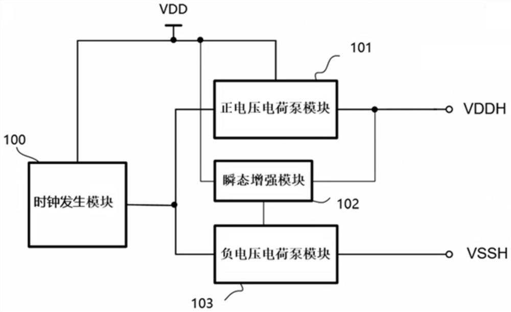
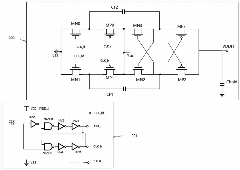
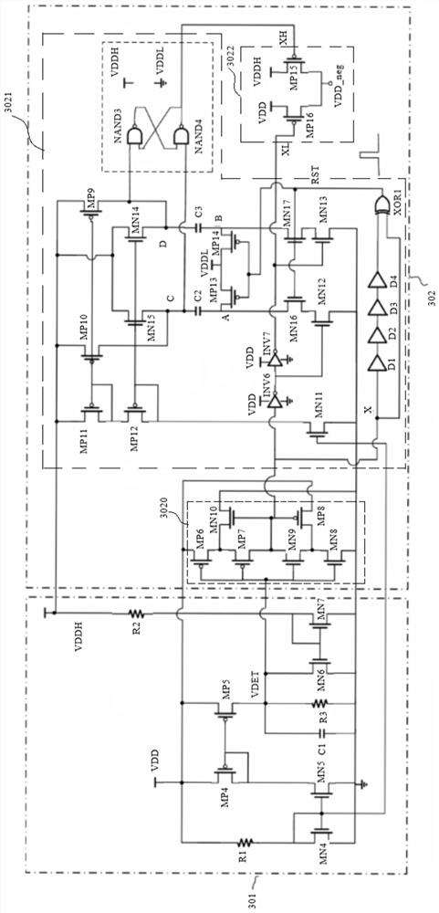
[0029] In order to be able to stably and reliably realize the output of a positive voltage higher than the positive rail of the input power supply voltage and a negative voltage lower than the negative rail of the input power supply voltage at the same time, and to enable the output negative voltage to be established flexibly and quickly, such as figure 1 As shown, the embodiment of the present invention provides a positive and negative voltage charge pump circuit, including a clock generation module 100 , a positive voltage charge pump module 101 , a transient enhancement module 102 and a negative voltage charge pump module 103 . The output end of the clock generation module 100 is connected to the input end of the positive voltage charge pump module 101 and the negative voltage charge pump module 103, the out...


PUM


Abstract

The invention discloses a positive and negative voltage charge pump circuit, a chip and a communication terminal. The positive and negative voltage charge pump circuit comprises a clock generation module, a positive voltage charge pump module, a transient enhancement module and a negative voltage charge pump module. The positive voltage charge pump module generates a positive voltage according toa clock signal output by a clock generation module, a transient enhancement module is adopted to sample the positive voltage and a power supply voltage and convert the positive voltage and the power supply voltage into a current for comparison, and a switchable input voltage is provided for a negative voltage charge pump module according to a comparison result. The negative voltage charge pump module not only can quickly and reliably establish negative voltage according to the clock signal output by the clock generation module so as to improve the negative voltage generation speed and efficiency of the negative voltage charge pump module, but also can flexibly meet the requirements of different negative voltages.

Description

technical field [0001] The invention relates to a positive and negative voltage charge pump circuit, and also relates to an integrated circuit chip including the positive and negative voltage charge pump circuit and a corresponding communication terminal, belonging to the technical field of analog integrated circuits. Background technique [0002] With the continuous improvement of integrated circuit integration, the continuous evolution of process nodes to the deep submicron limit, and the diversification of chip application environments, charge pump circuits, as a basic module circuit, are widely used in various integrated circuit products. The main function of the charge pump circuit is to provide the system with a positive voltage source higher than the positive rail of the input power supply voltage and a negative voltage source lower than the negative rail of the input power supply voltage, so as to better meet the system design specifications. Although positive power ...

Claims


Application Information

Patent Timeline
IPC IPC(8): H02M3/07
CPCH02M3/07H02M3/071H02M3/075H02M1/008
Inventor 王永寿陈成李春领林升
Owner SHANGHAI VANCHIP ELECTRONICS TECH CO LTD
Why Eureka
Try Eureka