Multi-chip bonding structure of LED semiconductor chip

A bonding structure, semiconductor technology, applied in semiconductor devices, semiconductor/solid-state device manufacturing, electrical components, etc., can solve the problems of long cooling time, LED chip cavity, LED chip heating, uneven cooling, etc., to reduce the heating time. and cooling time, increase bonding capacity, and shorten the effect of bonding time

Active Publication Date: 2021-02-26
河源市天和第三代半导体产业技术研究院
View PDF4 Cites 0 Cited by
  • Summary
  • Abstract
  • Description
  • Claims
  • Application Information

AI Technical Summary

Problems solved by technology

At present, the bonding fixture can only realize the single-chip bonding structure, and in the bonding process, the heating method is used to heat up and down the pressure head. This method of heating up and down by heating and bonding takes a long time to cool down and cannot conduct heat directly. On the semiconductor wafer, if the bonding structure heated by the upper and lower indenters is changed to multi-chip bonding, the LED chip will be heated and cooled unevenly due to the difference in heat conduction and heat dissipation of the semiconductor wafer or the bonding fixture, which will eventually lead to bond failure. The combined LED chip has problems such as voids, serious warping and fragments

Method used


Image

  • Multi-chip bonding structure of LED semiconductor chip
  • Multi-chip bonding structure of LED semiconductor chip
  • Multi-chip bonding structure of LED semiconductor chip

Examples


Embodiment Construction

[0029] In order to make the above objects, features and advantages of the present invention more comprehensible, the technical solutions of the present invention will be described in detail below in conjunction with the accompanying drawings and specific embodiments. It should be pointed out that the described embodiments are only a part of the embodiments of the present invention, rather than all embodiments. Based on the embodiments of the present invention, all those skilled in the art can obtain without creative work. Other embodiments all belong to the protection scope of the present invention.

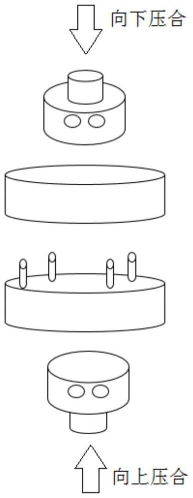
[0030] Traditional monolithic bonding structures such as figure 1 As shown, the current traditional bonding structure adopts the heating method of upper and lower indenters. This method cannot accurately control the entry temperature of each semiconductor wafer, and the production capacity is low. The semiconductor wafer carrier is an ordinary carrier without a heating plate.

...


PUM

PropertyMeasurementUnit
diameteraaaaaaaaaa

Abstract

The invention discloses a multi-chip bonding structure of an LED semiconductor chip. The multi-chip bonding structure comprises an upper pressure head, a lower pressure head, left and right positive and negative pole attaching blocks and semiconductor chip carriers, wherein the upper pressure head and the lower pressure head are connected with an oil pump or an air pump, can lift up and down, provide pressure and press semiconductor wafers in the carriers, and are both provided with cooling systems and temperature sensors so as to realize cooling of the semiconductor wafers in the carriers andreal-time transmission of the temperature of the pressure heads; each of the positive pole attaching block and the negative pole attaching block comprises a cooling system, a temperature sensor and an independent PID control system, so the current of each layer can be independently adjusted, and the temperature of each layer of a carrier pressing block can be controlled; a heating plate is arranged in each carrier, and the carriers can be stacked into a plurality of layers to realize synchronous bonding of a plurality of semiconductor wafers; and the heating plates of the carriers are in contact with the positive and negative pole attaching blocks, and after a power supply is switched on, the heating plates of the carriers can emit heat to heat the semiconductor wafers. According to the invention, multi-chip bonding can be realized, bonding time is shortened, and bonding capacity is increased.

Description

technical field [0001] The invention relates to the technical field of multi-chip bonding structures, in particular to a multi-chip bonding structure of LED semiconductor wafers. Background technique [0002] The LED semiconductor bonding method is a process of heating and pressing LED semiconductor wafers. [0003] In the MEMS process, the most commonly used are silicon-silicon direct bonding and silicon-glass electrostatic bonding technology, followed by a variety of new bonding technologies, such as metal-metal bonding technology. However, although various technologies continue to As it turns out, every technology has its drawbacks. [0004] The CB8 chip bonding machine manufactured by SUSS MicroTec in Germany has promoted the development of MEMS technology to a certain extent. However, problems such as poor bonding or chip breakage often occur in the manufacturing process. It is found through research that the existing technology is to be Bonding is performed when the ...

Claims


Application Information

Patent Timeline
Patent Type & Authority Applications(China)
IPC IPC(8): H01L33/00H01L21/67
CPCH01L21/67092H01L21/67098H01L33/005
Inventor 李国强
Owner 河源市天和第三代半导体产业技术研究院
Why Eureka
Try Eureka