Preparation method of horizontal ordered carbon nanotube array micro supercapacitor
A nanotube array and supercapacitor technology, which is applied in the field of preparation of on-chip horizontally ordered carbon nanotube array micro-supercapacitors, can solve the problem of not meeting the requirements of miniaturization, limiting the performance of micro-supercapacitors, and the difficulty of micro-supercapacitors. Capacitor preparation and other issues, to achieve the effect of improving fast charge and discharge capacity, reducing volume, and improving specific surface area utilization
- Summary
- Abstract
- Description
- Claims
- Application Information
AI Technical Summary
Problems solved by technology
Method used
Image
Examples
Embodiment 2
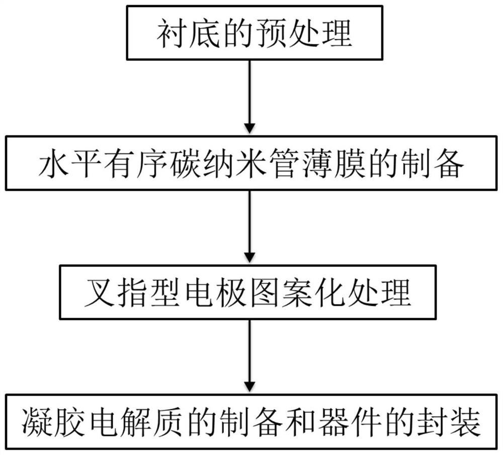
[0026] (1) First will have SiO 2 Thin Si substrate cut into 1 x 0.7cm 2 The slices were ultrasonically cleaned in acetone, ethanol and deionized water for 15 minutes to remove SiO 2 Organic matter or other impurities on the Si surface of the thin layer; then the cleaned SiO 2 The thin-layer Si substrate was etched in an oxygen plasma etching machine with a power of 300W and a vacuum of 120mTorr for 90s to make the surface hydrophilic.
[0027] (2) Treated with SiO 2 A thin layer of Si substrate was vertically inserted into a 2 μg / ml carbon nanotube dispersion, placed in a vacuum desiccator, and dried at 0.4 atm for 48 hours to obtain a horizontally ordered carbon nanotube film.
[0028] (3) The sample obtained in step (2) is spin-coated with a spin-coated photoresist (AZ5214) on the target substrate after the spin-coating parameter is 500r / s forward and then 4000r / s for 5s and 35s; Place on a heating plate at 90°C for 2 minutes to heat and dry; use a UV lithography machine...
Embodiment 3
[0033] (1) will first have SiO 2 Thin Si substrate cut into 1 x 0.7cm 2 The slices were ultrasonically cleaned in acetone, ethanol and deionized water for 15 minutes to remove SiO 2 Organic matter or other impurities on the Si surface of the thin layer; then the cleaned SiO 2 The thin-layer Si substrate was etched in an oxygen plasma etching machine with a power of 300W and a vacuum of 120mTorr for 90s to make the surface hydrophilic.
[0034] (2) Treated with SiO 2 A thin layer of Si substrate was vertically inserted into a 2 μg / ml carbon nanotube dispersion, placed in a vacuum desiccator, and dried at 0.4 atm for 48 hours to obtain a horizontally ordered carbon nanotube film.
[0035] (3) The sample obtained in step (2) is spin-coated with a spin-coated photoresist (AZ5214) on the target substrate after the spin-coating parameter is 500r / s forward and then 4000r / s for 5s and 35s; Place on a heating plate at 90°C for 2 minutes to heat and dry; use a UV lithography machine...
PUM
| Property | Measurement | Unit |
|---|---|---|
| size | aaaaa | aaaaa |
Abstract
Description
Claims
Application Information
 - Generate Ideas
- Intellectual Property
- Life Sciences
- Materials
- Tech Scout
- Unparalleled Data Quality
- Higher Quality Content
- 60% Fewer Hallucinations
Browse by: Latest US Patents, China's latest patents, Technical Efficacy Thesaurus, Application Domain, Technology Topic, Popular Technical Reports.
© 2025 PatSnap. All rights reserved.Legal|Privacy policy|Modern Slavery Act Transparency Statement|Sitemap|About US| Contact US: help@patsnap.com


