Cellular structure of power semiconductor device, and manufacturing method thereof
A technology for power semiconductors and manufacturing methods, which is applied in semiconductor/solid-state device manufacturing, semiconductor devices, electrical components, etc., can solve problems such as low channel mobility of MOSFET devices, increase channel carrier mobility, and increase yield , the effect of high pressure resistance
- Summary
- Abstract
- Description
- Claims
- Application Information
AI Technical Summary
Problems solved by technology
Method used
Image

Examples
no. 1 example
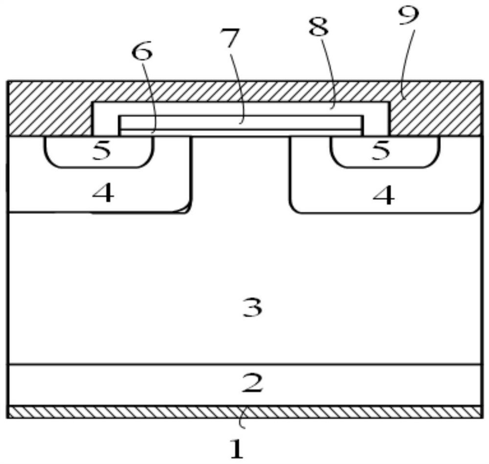
[0066] figure 2 is a schematic cross-sectional structure diagram of a power semiconductor device according to Embodiment 1 of the present invention;
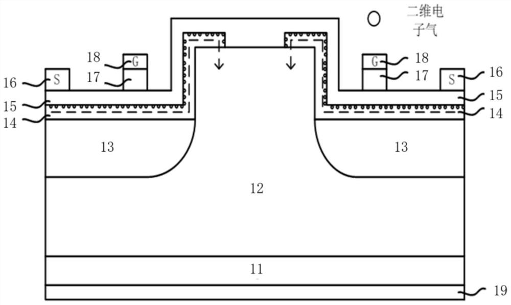
[0067] image 3 is a schematic diagram of a cross-sectional current path of a power semiconductor device according to Embodiment 1 of the present invention;
[0068] The power semiconductor device of this embodiment, such as figure 2 As shown, it includes: first conductivity type substrate 11, first conductivity type epitaxial layer 12, second conductivity type base region 13, channel layer 14, barrier layer 15, source metal 16, second conductivity type dielectric layer 17. Gate metal 18, drain metal 19.
[0069] The conductivity type adopted by each part in this embodiment can be set as the first conductivity type or the second conductivity type, and the first conductivity type and the second conductivity type are complementary conductivity types.
[0070] In this embodiment, the N type is set as the first conductivity ty...
no. 2 example
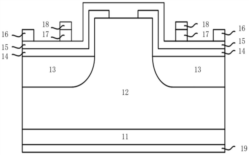
[0092] Figure 4 is a schematic cross-sectional structure diagram of the power semiconductor device of the present embodiment 2;
[0093] The power semiconductor device of this embodiment, such as Figure 4 As shown, it includes: drain metal 21, first conductivity type substrate 22, first conductivity type epitaxial layer 23, second conductivity type base region 24, channel layer 25, barrier layer 26, source metal 27, second conductivity type Two-conductivity type medium layer 28 , gate metal 29 , and metal layer 30 .
[0094] The conductivity type adopted by each part in this embodiment can be set as the first conductivity type or the second conductivity type, and the first conductivity type and the second conductivity type are complementary conductivity types.
[0095] In this embodiment, the N type is set as the first conductivity type, and the P type is set as the second conductivity type.
[0096] Wherein, the power semiconductor device includes a MOSFET or an IGBT, an...
no. 3 example
[0119] Figure 5 is a schematic cross-sectional structure diagram of the power semiconductor device of the present embodiment 3;
[0120] The power semiconductor device of this embodiment, such as Figure 5 As shown, it includes: drain metal 31, first conductivity type substrate 32, first conductivity type epitaxial layer 33, second conductivity type base region 34, channel layer 35, barrier layer 36, source metal 37, second conductivity type Two-conductivity type dielectric layer 38 and gate metal 39 .
[0121] The conductivity type adopted by each part in this embodiment can be set as the first conductivity type or the second conductivity type, and the first conductivity type and the second conductivity type are complementary conductivity types.
[0122] In this embodiment, the N type is set as the first conductivity type, and the P type is set as the second conductivity type.
[0123] Wherein, the power semiconductor device includes a MOSFET or an IGBT, and this embodime...
PUM
| Property | Measurement | Unit |
|---|---|---|
| thickness | aaaaa | aaaaa |
| thickness | aaaaa | aaaaa |
| electrical resistivity | aaaaa | aaaaa |
Abstract
Description
Claims
Application Information
 - R&D
- Intellectual Property
- Life Sciences
- Materials
- Tech Scout
- Unparalleled Data Quality
- Higher Quality Content
- 60% Fewer Hallucinations
Browse by: Latest US Patents, China's latest patents, Technical Efficacy Thesaurus, Application Domain, Technology Topic, Popular Technical Reports.
© 2025 PatSnap. All rights reserved.Legal|Privacy policy|Modern Slavery Act Transparency Statement|Sitemap|About US| Contact US: help@patsnap.com