Preparation method of mos device and mos device

A MOS device and substrate technology, applied in the field of crystals, can solve problems such as increased interface state density, carrier transport interface scattering, and impact on interface quality, so as to avoid high-temperature processes, improve carrier mobility characteristics, and improve Effect of Gate Oxide Reliability

Active Publication Date: 2022-02-18
INST OF SEMICONDUCTORS - CHINESE ACAD OF SCI
View PDF0 Cites 0 Cited by
  • Summary
  • Abstract
  • Description
  • Claims
  • Application Information

AI Technical Summary

Problems solved by technology

At the same time, when the Si element is incompletely oxidized, it is easy to form the secondary oxide and interface state of Si at the interface, which seriously affects the SiO 2 / SiC interface quality, resulting in SiC and SiO 2 The increase of the interface state density has formed serious interface scattering for the carrier transport of SiC-based MOS devices

Method used


Image

  • Preparation method of mos device and mos device
  • Preparation method of mos device and mos device
  • Preparation method of mos device and mos device

Examples


Embodiment Construction

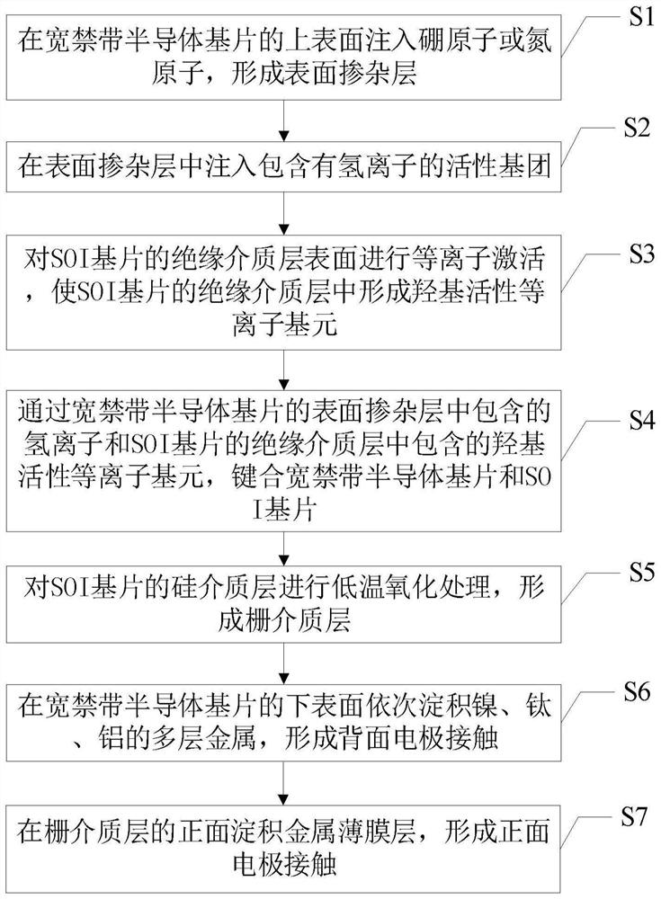
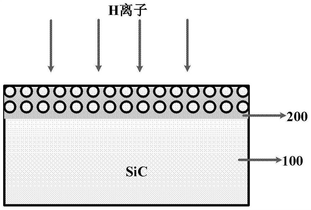
[0042] In order to make the purpose, features, and advantages of the application more obvious and understandable, the technical solutions in the embodiments of the application will be clearly and completely described below in conjunction with the drawings in the embodiments of the application. Obviously, the described The embodiments are only some of the embodiments of the present application, but not all of them. Based on the embodiments in this application, all other embodiments obtained by those skilled in the art without making creative efforts belong to the scope of protection of this application.

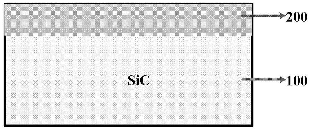
[0043] figure 1 It is a flowchart of the preparation method of the MOS device provided by the present disclosure. The MOS device includes a wide bandgap semiconductor substrate 100 and an SOI (Silicon-On-Insulator) substrate, and the SOI substrate includes a silicon dielectric layer 400 and an insulating dielectric layer 300 .

[0044] Such as figure 1 Shown, this preparati...


PUM

PropertyMeasurementUnit
thicknessaaaaaaaaaa
thicknessaaaaaaaaaa

Abstract

The present disclosure provides a method for preparing a MOS device and a MOS device. The MOS device includes a wide bandgap semiconductor substrate and an SOI substrate, and the wide bandgap semiconductor substrate is made of silicon carbide, gallium nitride, gallium oxide, or diamond. Any one of the methods, the method includes: implanting boron or nitrogen atoms on the upper surface of the wide bandgap semiconductor substrate to form a surface doped layer; implanting active groups containing hydrogen ions into the surface doped layer; Plasma activation is performed on the surface of the insulating dielectric layer of the sheet to form a hydroxyl active plasma unit in the insulating dielectric layer; through the hydrogen ions contained in the surface doping layer and the hydroxyl active plasma unit contained in the insulating dielectric layer, the wide band gap is bonded For semiconductor substrates and SOI substrates, perform low-temperature oxidation treatment on the silicon dielectric layer to form a gate dielectric layer; sequentially deposit multi-layer metals of nickel, titanium, and aluminum on the lower surface of the wide-bandgap semiconductor substrate to form a back electrode contact; A metal thin film layer is deposited on the front surface of the gate dielectric layer to form a front electrode contact.

Description

technical field [0001] The present application relates to the field of crystal technology, in particular to a method for preparing a MOS device and the MOS device. Background technique [0002] Silicon carbide (SiC) is a wide bandgap semiconductor with excellent performance. It not only has a wide band gap (3 times that of silicon), high thermal conductivity (3.3 times that of silicon), and high breakdown field strength (10 times that of silicon). , Saturated electron drift rate is high (2.5 times that of silicon), and it also has excellent physical and chemical stability, strong radiation resistance and mechanical strength, etc. It is the material of choice for high-power power electronic devices. Therefore, electronic devices based on wide-bandgap SiC materials can be used in power electronics fields such as high temperature, high power, high frequency, and high radiation, and can give full play to the important advantages and outstanding features of SiC-based devices in t...

Claims


Application Information

Patent Timeline
Patent Type & Authority Patents(China)
IPC IPC(8): H01L29/423H01L29/16H01L29/78H01L21/336
CPCH01L29/42364H01L29/1608H01L29/7827H01L29/66666
Inventor 申占伟刘兴昉赵万顺王雷闫果果孙国胜曾一平
Owner INST OF SEMICONDUCTORS - CHINESE ACAD OF SCI
Why Eureka
Try Eureka