Power chip preparation method and power chip
A power chip and drift layer technology, which is applied in semiconductor/solid-state device manufacturing, electrical components, circuits, etc., can solve problems such as complex processes, achieve simple processes, improve over-current shutdown capabilities, and reduce electric field strength.
- Summary
- Abstract
- Description
- Claims
- Application Information
AI Technical Summary
Problems solved by technology
Method used
Image
Examples
Embodiment 1
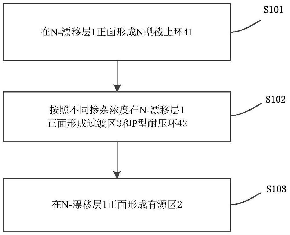
[0055] Embodiment 1 of the present invention provides a method for preparing a power chip, the specific flow chart is as follows figure 1 As shown, the specific process is as follows:
[0056] S101: forming an N-type stop ring 41 on the front of the N-drift layer 1;
[0057] S102: Form a transition region 3 and a P-type withstand voltage ring 42 on the front of the N-drift layer 1 according to different doping concentrations;
[0058] S103: forming an active region 2 on the front surface of the N-drift layer 1;
[0059] The doping concentration of the transition region 3 near the active region 2 is greater than the doping concentration near the P-type voltage-sustaining ring 42 , and the doping depth of the transition region 3 near the active region 2 is greater than the doping depth near the P-type voltage-sustaining ring 42 .
[0060] Among them, the resistivity and thickness parameters of the N-material used in the N-drift layer 1 are closely related to the breakdown volta...
Embodiment 2
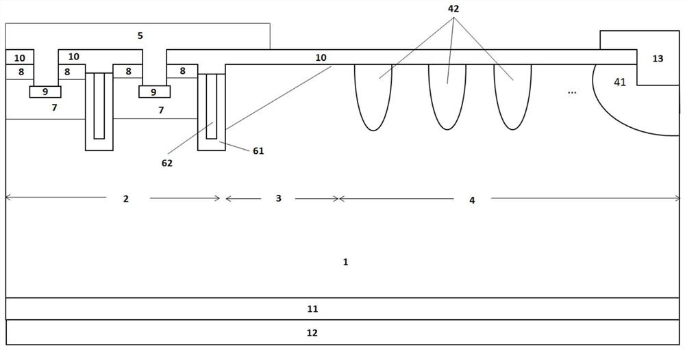
[0094] Embodiment 2 of the present invention provides a power chip prepared by using the power chip preparation method of Embodiment 1, such as figure 2 As shown, it includes an N-drift layer 1, an active region 2, a transition region 3, an N-type stop ring 41 and a P-type voltage-resistant ring 42; the N-type stop ring 41 and the P-type voltage-resistant ring 42 form a terminal region 4;
[0095] The active region 2, the transition region 3, the N-type stop ring 41 and the P-type voltage-resistant ring 42 are all located on the front of the N-drift layer 1, the N-type stop ring 41 is located at the edge of the N-drift layer 1, and the P-type voltage-resistant ring 42 is located between the transition zone 2 and the N-type stop ring 41;
[0096] The transition region 3 is formed according to different doping concentrations, and the doping concentration of the transition region 3 close to the active region 2 is greater than the doping concentration close to the P-type withstan...
PUM
| Property | Measurement | Unit |
|---|---|---|
| thickness | aaaaa | aaaaa |
| thickness | aaaaa | aaaaa |
Abstract
Description
Claims
Application Information
 - R&D Engineer
- R&D Manager
- IP Professional
- Industry Leading Data Capabilities
- Powerful AI technology
- Patent DNA Extraction
Browse by: Latest US Patents, China's latest patents, Technical Efficacy Thesaurus, Application Domain, Technology Topic, Popular Technical Reports.
© 2024 PatSnap. All rights reserved.Legal|Privacy policy|Modern Slavery Act Transparency Statement|Sitemap|About US| Contact US: help@patsnap.com


