A microwave biosensor applied to healthy-iot and its preparation method
A sensor and seed technology, applied in the field of physical analysis devices for biological substances, can solve the problems of low sensitivity, large size, and low quality factor, and achieve the effects of solving low sensitivity, reducing chip size, and improving quality factor.
- Summary
- Abstract
- Description
- Claims
- Application Information
AI Technical Summary
Problems solved by technology
Method used
Image
Examples
Embodiment 1
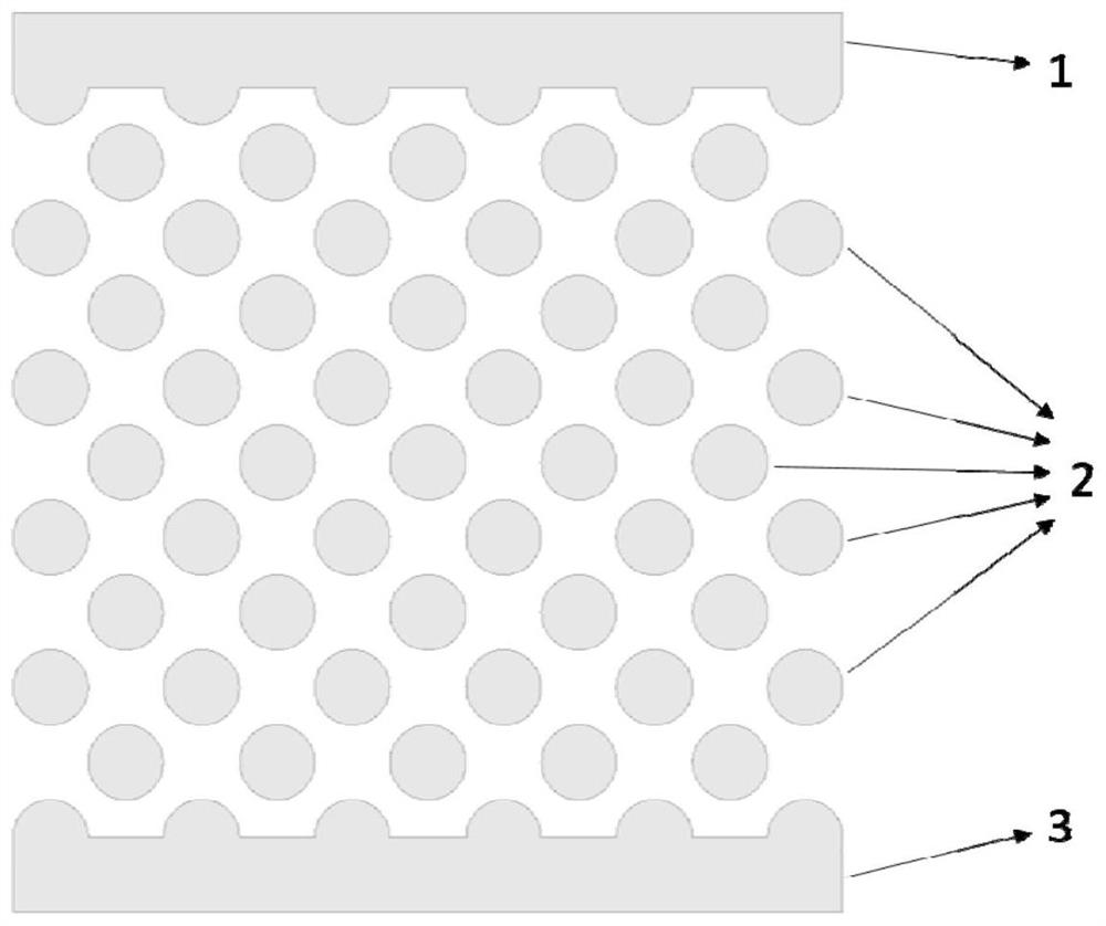
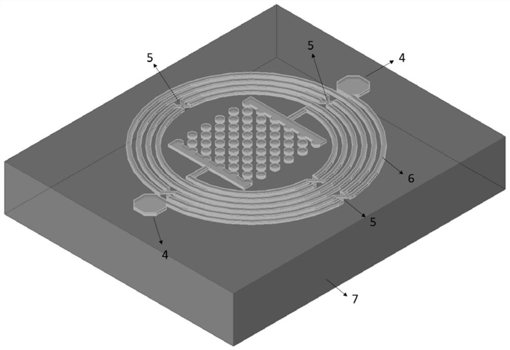
[0025] a sensor such as figure 2 As shown, including the wafer as the bearing reference, at least two measurement Pad points are set on the surface of the wafer. In this embodiment, two measurement Pad points are set on the wafer, and the two measurement Pad points are represented by the wafer The center of is the symmetric datum, which is set symmetrically on both sides of the wafer center point. An area is reserved between the two measurement pad points, and a differential inductance coil is set in the reserved area, and several air bridge structures are arranged on the differential inductance coil, and the air bridge structure ring array is on the differential inductance coil, in this embodiment , there are five air bridge structures, two of which are just aligned with the measurement pad point.
[0026] In the area surrounded by the differential inductance coil, there is also a point array capacitor. The point array array contains several point capacitors. All the capaci...
Embodiment 2
[0028] A method for preparing a sensor, comprising the steps of:
[0029] Step (1): Use plasma to clean the surface of the GaAs wafer; the specific cleaning process is: sequentially wash with acetone Acetone, isopropanol IPA and deionized water DI-water, and then use hydrochloric acid solution HCl / H 2 O chemically polishes the wafer.
[0030] Step (2): Using plasma-enhanced chemical vapor deposition equipment, deposit a gallium nitride dielectric layer on the surface of the GaAs wafer. In this embodiment, the thickness of the dielectric layer ranges from 190-210 microns, and the optional endpoint value is 190mm , 210mm, the middle value is 200mm;
[0031] Step (3): Ti / Au is sputtered onto the surface by metal sputtering equipment as the first layer of seed metal; the thickness of the seed metal is 20 / 80 nanometers of Ti / Au.
[0032] Step (4): Based on the first photomask, use photoresist to define the required structure of the underlying metal, and use the solution replaceme...
Embodiment 3
[0039] A microwave biosensor with high sensitivity applied to Healthy-IoT, when designing, use Advanced Design System 2015 software on the computer to design and simulate a compact microwave LC resonator; The detection of the concentration of the biomarker solution can be completed by dropping the micro-upgraded biomarker solution in the area where the point array capacitor is located; when the concentration of the biomarker solution changes, the dielectric constant of the biomarker solution itself also changes, and the two Therefore, the biomarker solutions with different concentrations will have different effects on the electromagnetic field characteristics of the microwave resonator device after being dropped into the capacitance area, so that the parameter characteristics of the microwave device will also change accordingly. The microwave LC type resonator proposed by the present invention is just by detecting the center frequency of the microwave resonator device, thereby ...
PUM
| Property | Measurement | Unit |
|---|---|---|
| thickness | aaaaa | aaaaa |
| thickness | aaaaa | aaaaa |
| thickness | aaaaa | aaaaa |
Abstract
Description
Claims
Application Information
 - R&D
- Intellectual Property
- Life Sciences
- Materials
- Tech Scout
- Unparalleled Data Quality
- Higher Quality Content
- 60% Fewer Hallucinations
Browse by: Latest US Patents, China's latest patents, Technical Efficacy Thesaurus, Application Domain, Technology Topic, Popular Technical Reports.
© 2025 PatSnap. All rights reserved.Legal|Privacy policy|Modern Slavery Act Transparency Statement|Sitemap|About US| Contact US: help@patsnap.com


