A 3D display-oriented micro-led with a vertical structure for emitting circularly polarized light and its preparation method
A technology of circularly polarized light and vertical structure, applied in semiconductor devices, electrical components, circuits, etc., can solve problems such as inconvenient viewing, achieve good temperature stability, improve signal stability, and improve light extraction efficiency
- Summary
- Abstract
- Description
- Claims
- Application Information
AI Technical Summary
Problems solved by technology
Method used
Image
Examples
Embodiment 1
[0053] The structure of the vertical structure Micro-LED facing 3D display in the present invention is as follows: Figure 10 As shown, the Micro-LED chip includes a micro-nano structure layer 12, a dielectric film layer 10, an n-GaN layer 3, an MQW layer 4, a p-GaN layer 5, a conductive layer 6 and a grating layer 7 from top to bottom; n- The width of GaN layer 3, MQW layer 4, p-GaN layer 5 is equal, the width of conductive layer 6 is equal to the width of grating layer 7; The width of dielectric film layer 10 is smaller than n-GaN layer 3, on the n-GaN layer The mesa 11 will leak out on both sides; the width of the grating is greater than that of the n-GaN layer 3, the MQW layer 4, and the p-GaN layer 5, and the mesa 11 will leak out on both sides of the conductive layer 6, and the n-GaN layer 3, the MQW layer 4, the p- The GaN layer 5 leaks two sidewalls; there is a passivation layer 8 on the mesa 11 and the sidewall; the shape of the passivation layer 8 is a right-angled Z...
Embodiment 2
[0055] The preparation method of the vertical structure Micro-LED that emits circularly polarized light for 3D display in the blue light area provided in this embodiment includes the following steps:
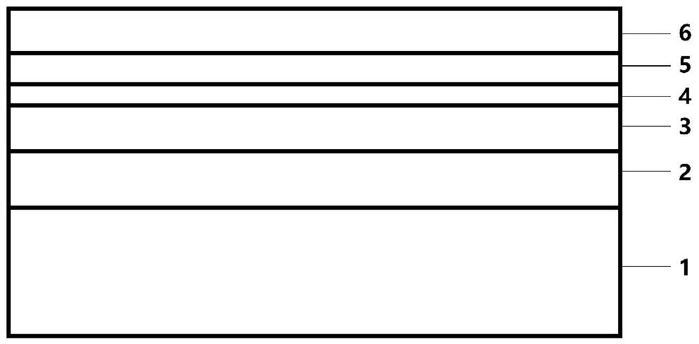
[0056] (1) On the (0001) plane sapphire (substrate 1), grow u-GaN layer 2 (5 μm in thickness), n-GaN layer 3 (5 μm in thickness), [InGaN (2nm) / GaN (10nm)] 8 MQW (quantum well) layer 4 (thickness is 96nm), p-GaN layer 5 (thickness is 100nm), obtains LED epitaxy material, the mass percentage content of In composition in MQW (InGaN quantum well) layer 4 is 15%, in In this embodiment, the emission wavelength is 470nm, which belongs to the blue light region. The structure of the obtained LED epitaxial material in step (1) is as follows: figure 1 shown.
[0057] (2) Fabricate the conductive layer 6 on the p-GaN layer 5 by means of electron beam evaporation, wherein the deposition temperature is 220° C., the conductive layer is ITO, and the thickness of the conductive layer 6 is 280...
Embodiment 3
[0068] The preparation method of the vertical microcavity GaN-based Micro-LED with the green light area facing the display and emitting circularly polarized light provided in this embodiment includes the following steps:
[0069] (1) First, grow u-GaN layer 2 (5 μm in thickness), n-GaN layer 3 (5 μm in thickness), [InGaN (2 nm) / GaN ( 10nm)] 8 MQW (quantum well) layer 4 (thickness: 96nm), p-GaN layer 5 (thickness: 100nm), to obtain LED epitaxial material. The mass percentage of In in the MQW (InGaN quantum well) layer 4 is 28%. In this embodiment, the emission wavelength is 530nm, which belongs to the green light region. The structure of the obtained LED epitaxial material in step (1) is as follows: figure 1 shown.
[0070] (2) The conductive layer 6 is fabricated on the p-GaN layer 5 by means of electron beam evaporation, wherein the deposition temperature is 220° C., the conductive layer is ITO, and the thickness of the conductive layer 6 is 280 nm. The structure obtained...
PUM
| Property | Measurement | Unit |
|---|---|---|
| size | aaaaa | aaaaa |
| thickness | aaaaa | aaaaa |
| thickness | aaaaa | aaaaa |
Abstract
Description
Claims
Application Information
 - R&D
- Intellectual Property
- Life Sciences
- Materials
- Tech Scout
- Unparalleled Data Quality
- Higher Quality Content
- 60% Fewer Hallucinations
Browse by: Latest US Patents, China's latest patents, Technical Efficacy Thesaurus, Application Domain, Technology Topic, Popular Technical Reports.
© 2025 PatSnap. All rights reserved.Legal|Privacy policy|Modern Slavery Act Transparency Statement|Sitemap|About US| Contact US: help@patsnap.com


