Solder resist hole plugging method for BMU printed circuit board

A technology for printed circuit boards and plug holes, which is applied in the fields of printed circuit, printed circuit, and printed circuit manufacturing. Effect

Active Publication Date: 2020-11-24
TEAN ELECTRONICS DA YA BAY CO LTD
View PDF4 Cites 1 Cited by
  • Summary
  • Abstract
  • Description
  • Claims
  • Application Information

AI Technical Summary

Problems solved by technology

[0008] The purpose of the present invention is to provide a BMU printed circuit board solder resistance plugging method to solve the technical problem that the plug hole is not full when the BMU printed circuit board has solder resistance plugging in the prior art

Method used


Image

  • Solder resist hole plugging method for BMU printed circuit board

Examples


Embodiment Construction

[0043] The following will clearly and completely describe the technical solutions in the embodiments of the present invention in conjunction with the accompanying drawings in the embodiments of the present invention, but this does not constitute a limitation to the protection scope of the present invention.

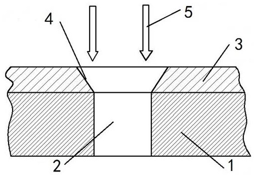
[0044] see figure 1 , The present embodiment provides a BMU printed circuit board 1 solder resist plugging method, comprising the following steps:

[0045] S1. Targeting: Target holes are made on the BMU printed circuit board 1; in actual operation, the target holes can be made on the BMU printed circuit board 1 by a shooting machine, and the significance of the target holes is that the BMU printed circuit board 1 usually consists of many layers of plates Stacking and pressing together requires target holes for alignment, so that the alignment accuracy can meet the production needs, otherwise the misalignment between layers will lead to open circuits and affect reliabilit...


PUM


Abstract

The invention discloses a solder resist hole plugging method for a BMU printed circuit board. The solder resist hole plugging method comprises the following steps of: S1, target shooting; S2, edges and fillets milling; S3, acid etching for copper reduction; S4, board grinding; S5, selective plating, so that an annular slope is formed in the region, close to the hole position, of the hole needing solder mask hole plugging; S6, sequentially subjecting a BMU printed circuit board to drilling, copper deposition, board electroplating, line pretreatment, film pressing, exposure, development, detection, pattern electroplating, alkaline etching and AOI; and S7, sequentially carrying out solder mask hole plugging, surface oil printing, pre-baking, exposure and development on the BMU printed circuitboard. The solder resist hole plugging method is reasonable in step design, the steps S3, S4 and S5 are added, and an annular slope is formed in the region, close to the step S3, S4 and S5, of the hole site needing solder mask hole plugging, so that the plumpness of the plugged hole is improved, ink rising is avoided, and yellowing of the via hole is avoided.

Description

technical field [0001] The invention relates to the technical field of printed circuit board production, in particular to a method for plugging holes of a BMU printed circuit board with solder resistance. Background technique [0002] The BMU is a car battery board, and there are many vias on the BMU printed circuit board, which usually need to be soldered and plugged. However, in the production process of solder mask plugging these vias, there are the following problems: [0003] (1) Because the hole diameter of the via hole that needs to be soldered and plugged is relatively small, only 0.5mm, but the surface copper thickness on the BMU printed circuit board is as high as 4OZ (where the thickness of 1OZ copper foil = 35um), the BMU printed circuit board The thickness of the board itself is as high as 6.2mm, and the ink itself has a certain tension. As a result, when these vias are plugged with solder mask, the plug holes will not be full. [0004] (2) When pre-baking and...

Claims


Application Information

Patent Timeline
IPC IPC(8): H05K3/00
CPCH05K3/0094H05K2201/0959
Inventor 王康兵周刚
Owner TEAN ELECTRONICS DA YA BAY CO LTD
Why Eureka
Try Eureka