Perovskite solar cell based on down-conversion layer and preparation method of perovskite solar cell
A solar cell and perovskite technology, applied in the field of solar cells, can solve the problems of decreased efficiency of perovskite solar cells, affecting electron transport performance, energy level mismatch, etc., so as to improve the photoelectric conversion ability, avoid performance decline, improve The effect of absorption properties
- Summary
- Abstract
- Description
- Claims
- Application Information
AI Technical Summary
Problems solved by technology
Method used
Image
Examples
Embodiment 1
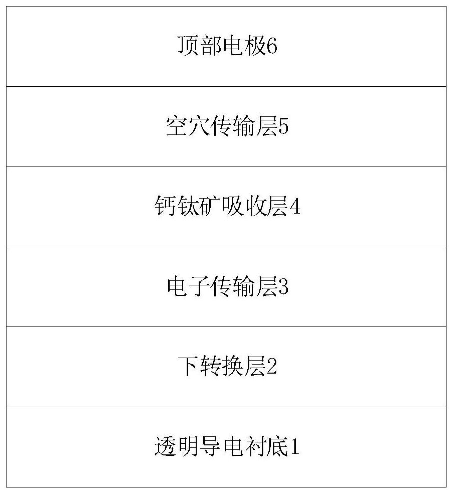
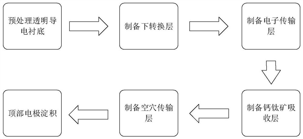
[0042] Example 1: Preparation of transparent conductive substrate using indium tin oxide ITO, down conversion layer using gadolinium nitrate doped with dysprosium, electron transport layer using tin oxide, perovskite light absorbing layer using MAPbI 3 , the hole transport layer is made of 2,2',7,7'-tetrakis[N,N-bis(4-methoxyphenyl)amino]-9,9'-spirobifluorene material, and the top electrode is made of silver Ag perovskite solar cells.
[0043] The first step is to pretreat the indium tin oxide ITO transparent conductive substrate.
[0044] 1.1) Use industrial cleaner Decon-90 aqueous solution, deionized water, acetone, and isopropanol solution to ultrasonically clean the ITO transparent conductive substrate with a specification of 10Ω / sq indium tin oxide step by step at 50°C. The ultrasonic cleaning time of the agent is 20min, and then use a nitrogen gun to dry the surface of the cleaned indium tin oxide ITO transparent conductive substrate;
[0045]1.2) Use ultraviolet ozon...
Embodiment 2
[0062] Example 2: Preparation of a transparent conductive substrate using indium tin oxide ITO, gadolinium vanamate doped with europium for the down conversion layer, zinc oxide for the electron transport layer, and MA for the perovskite light absorbing layer 1-y FA y PB 3-x Cl x , the hole transport layer uses cuprous thiocyanate, and the top electrode uses a perovskite solar cell with a carbon electrode.
[0063] Step 1, pretreating the indium tin oxide ITO transparent conductive substrate.
[0064] The specific implementation of this step is the same as the first step of Example 1.
[0065] Step 2, preparing a dysprosium-doped lanthanum acetate down conversion layer.
[0066] 2a) Add 30 mg of ammonium vanadate and 300 mg of sodium hydroxide into 2.5 ml of deionized water to obtain a sodium vanadate solution. Add 5 mL of oleic acid and 5 mL of ethanol to the above sodium vanadate solution;
[0067] 2b) adding a solution of 340 mg lanthanum acetate hexahydrate and 40 mg...
Embodiment 3
[0082] Example 3: Preparation of a transparent conductive substrate using fluorine-doped tin oxide FTO, the down conversion layer using gadolinium oxide doped with europium, and the electron transport layer using TiO 2 , the perovskite light absorbing layer adopts MA 1-y FA y PB 3 , the hole transport layer uses poly[bis(4-phenyl)(2,4,6-trimethylphenyl)amine] material, and the top electrode uses gold Au perovskite solar cells.
[0083] Step A, pretreating the fluorine-doped tin oxide FTO transparent conductive substrate.
[0084] Firstly, use industrial cleaning agent Decon-90 aqueous solution, deionized water, acetone, and isopropanol solution to ultrasonically clean the FTO transparent conductive substrate with a specification of 15Ω / sq fluorine-doped tin oxide step by step at 50°C. The ultrasonic cleaning time of the agent is 20min, and the surface of the cleaned fluorine-doped tin oxide FTO transparent conductive substrate is dried with a nitrogen gun;
[0085] Then, t...
PUM
 Abstract
Description
Claims
Application Information
 - Generate Ideas
- Intellectual Property
- Life Sciences
- Materials
- Tech Scout
- Unparalleled Data Quality
- Higher Quality Content
- 60% Fewer Hallucinations
Browse by: Latest US Patents, China's latest patents, Technical Efficacy Thesaurus, Application Domain, Technology Topic, Popular Technical Reports.
© 2025 PatSnap. All rights reserved.Legal|Privacy policy|Modern Slavery Act Transparency Statement|Sitemap|About US| Contact US: help@patsnap.com


