LED chip packaging structure
A technology of LED chip and packaging structure, applied in the direction of semiconductor devices, electrical components, circuits, etc., can solve the problems of uneven light output, yellow edge, weak light efficiency, etc., and achieve the effect of improving light output efficiency
- Summary
- Abstract
- Description
- Claims
- Application Information
AI Technical Summary
Problems solved by technology
Method used
Image
Examples
Embodiment Construction
[0026] The scheme of this application is further described in conjunction with the accompanying drawings as follows:
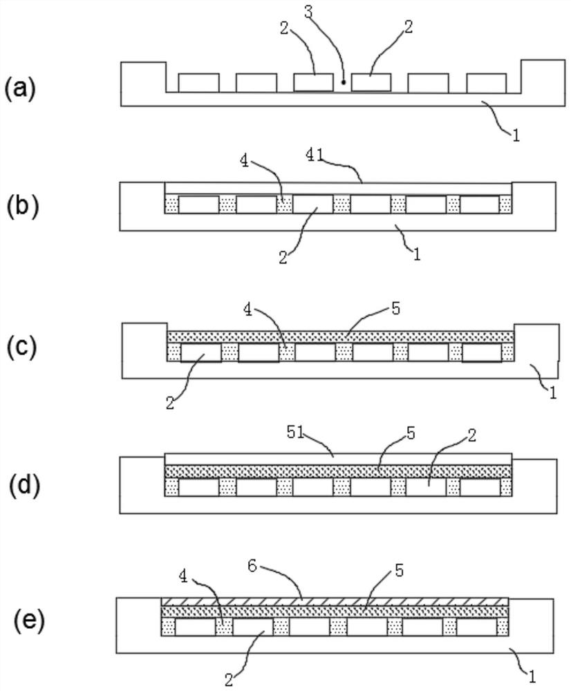
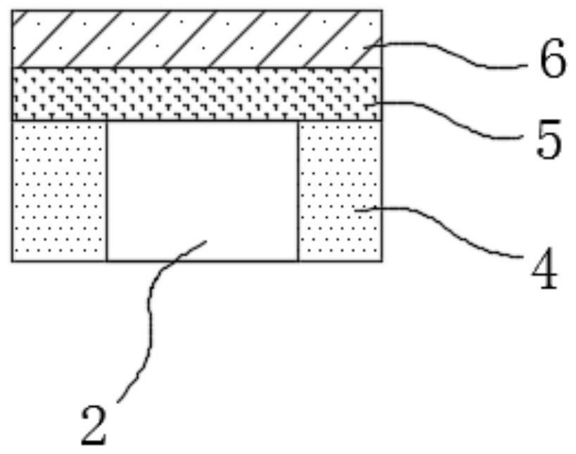
[0027] Such as figure 1 As shown, a LED chip packaging structure includes an LED chip 2, a first fluorescent adhesive layer 4 is provided on the peripheral side of the LED chip 2, and a second fluorescent adhesive layer 5 is provided on the top surface of the LED chip 2. A protective film layer 6 is disposed on the second fluorescent glue layer 5 .
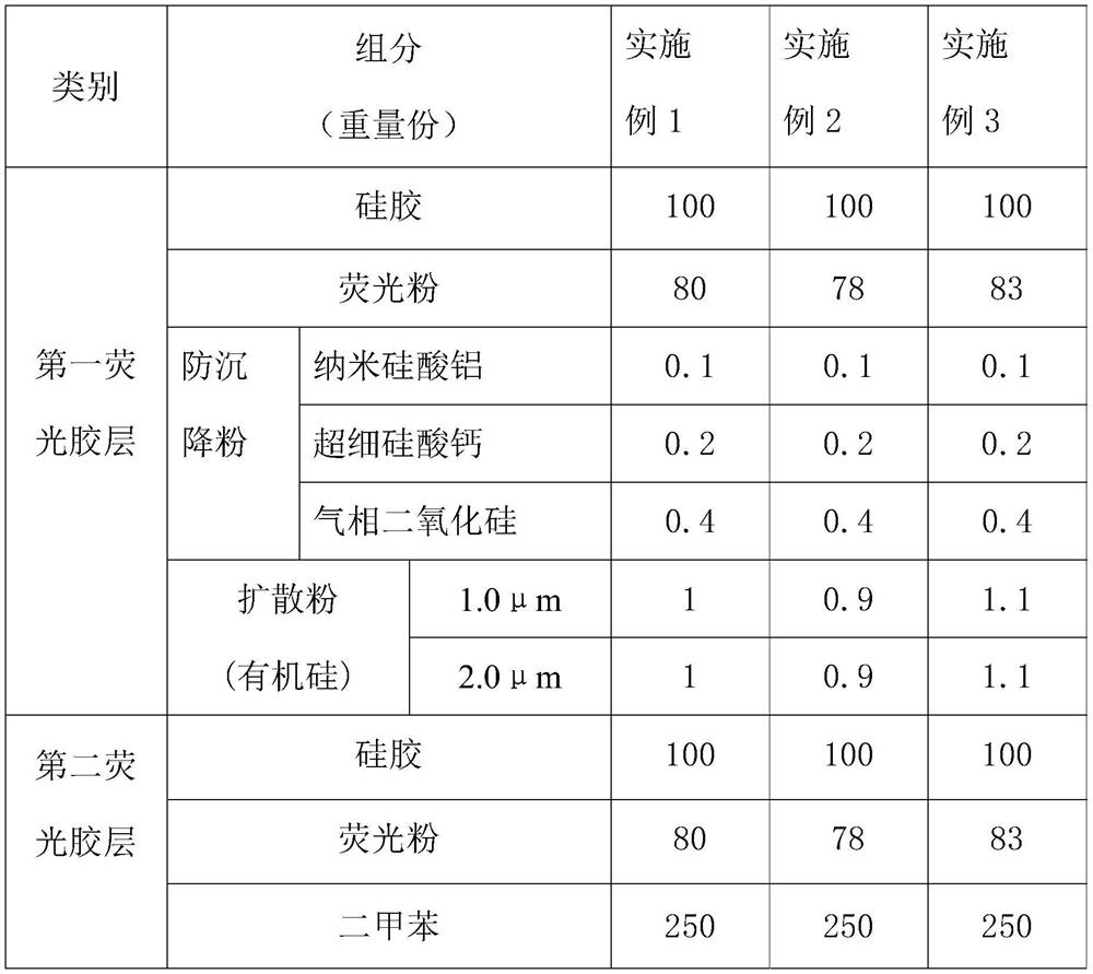
[0028] The first fluorescent glue layer 4 includes the following components by weight:
[0029] Silica gel: 85-115 parts by weight;
[0030] Phosphor powder: 76-83 parts by weight;
[0031] Anti-sedimentation powder: 0.3 to 0.8 parts by weight;
[0032] Diffusion powder: 1 to 3 parts by weight.
[0033] The anti-sedimentation powder includes nano-aluminum silicate, superfine calcium silicate and fumed silica, and the mass ratio of the nano-aluminum silicate, superfine calcium silicate and fumed silica is (1-1...
PUM
| Property | Measurement | Unit |
|---|---|---|
| Particle size | aaaaa | aaaaa |
Abstract
Description
Claims
Application Information
 - Generate Ideas
- Intellectual Property
- Life Sciences
- Materials
- Tech Scout
- Unparalleled Data Quality
- Higher Quality Content
- 60% Fewer Hallucinations
Browse by: Latest US Patents, China's latest patents, Technical Efficacy Thesaurus, Application Domain, Technology Topic, Popular Technical Reports.
© 2025 PatSnap. All rights reserved.Legal|Privacy policy|Modern Slavery Act Transparency Statement|Sitemap|About US| Contact US: help@patsnap.com


