Flexible thin film packaged OLED structure and manufacturing method

A flexible film and manufacturing method technology, applied in semiconductor/solid-state device manufacturing, electrical components, electrical solid-state devices, etc., can solve the problems of ink flow, easy separation, uneven ink diffusion, etc., to reduce warpage and ease side edges The effect of stress concentration

Pending Publication Date: 2020-11-17
FUJIAN HUAJIACAI CO LTD
View PDF6 Cites 1 Cited by
  • Summary
  • Abstract
  • Description
  • Claims
  • Application Information

AI Technical Summary

Problems solved by technology

[0009] The contact surface characteristics of organic and inorganic substances in flexible packaging are different, the adhesion between the contact surfaces is poor, and it is easy to form water / oxygen penetration on the side of the film, and when IJP prepares the organic layer, due to the coffee ring effect of the ink and The Marangoni effect leads to abnormal phenomena such as uneven ink diffusion, uneven edges, and ink flow. The existing common technology uses a barrier wall to prevent ink flow, but the barrier wall and the inorganic film have poor adhesion and are easy to separate, resulting in side effects. Encapsulation failure due to water / oxygen penetration at the edge affects the life of OLED devices

Method used


Image

  • Flexible thin film packaged OLED structure and manufacturing method
  • Flexible thin film packaged OLED structure and manufacturing method
  • Flexible thin film packaged OLED structure and manufacturing method

Examples


Embodiment 1

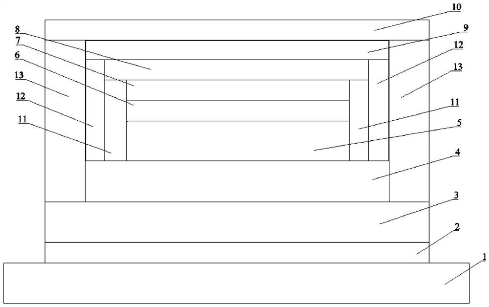
[0072] Please refer to Figure 1 to Figure 2 , Embodiment 1 of the present invention is:

[0073] A flexible film-encapsulated OLED structure, comprising a glass substrate 1, a first inorganic partition wall 13, an organic partition wall 12, a second inorganic partition wall 11, and a first inorganic thin film layer 3 stacked sequentially above the glass substrate 1 from bottom to top , the first organic thin film layer 4, the OLED assembly, the buffer layer 7, the second inorganic thin film layer 8, the second organic thin film layer 9 and the third inorganic thin film layer 10;

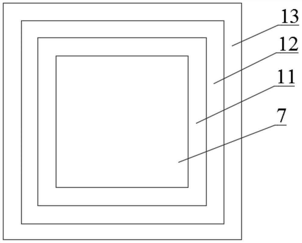
[0074] Wherein, the second inorganic partition wall 11 wraps the sides of the OLED assembly and the buffer layer 7, and is located between the first organic thin film layer 4 and the second inorganic thin film layer 8, and the organic partition wall 12 wraps the second inorganic partition wall 11 and the side of the second inorganic thin film layer 8, and between the first organic thin film layer 4...

Embodiment 2

[0078] Please refer to Figure 1 to Figure 2 , the second embodiment of the present invention is:

[0079] A flexible film-encapsulated OLED structure, further comprising a silicon dioxide film layer 2 on the basis of the first embodiment above;

[0080] The silicon dioxide thin film layer 2 is located between the glass substrate 1 and the first inorganic thin film layer 3 , and the thickness of the silicon dioxide thin film layer 2 ranges from 0.2um to 0.4um, preferably 0.3um.

Embodiment 3

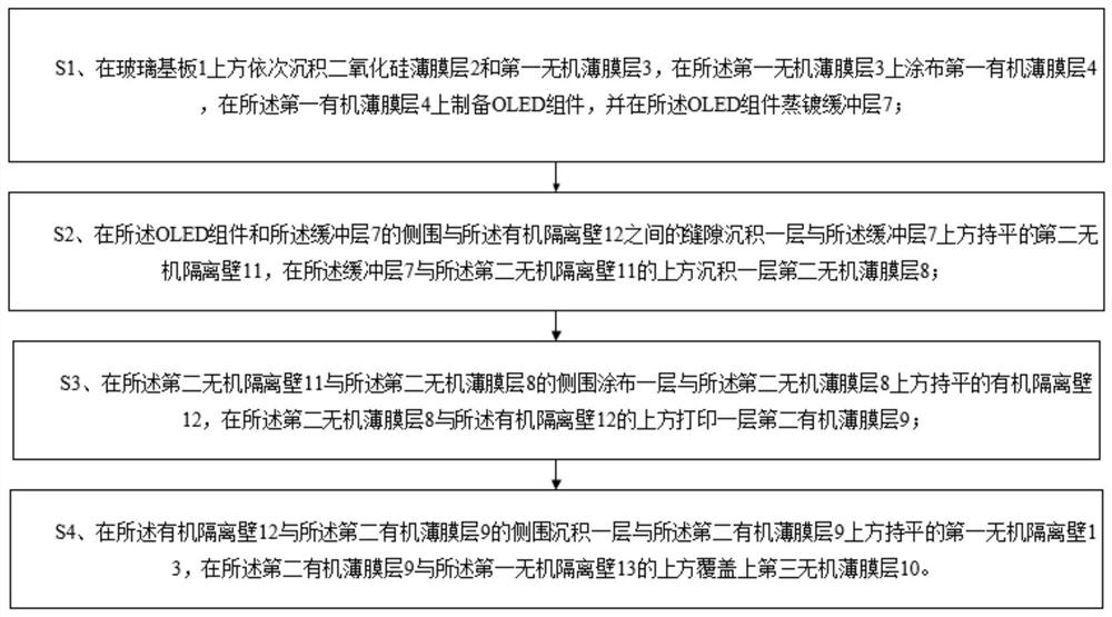
[0081] Please refer to image 3 , Embodiment three of the present invention is:

[0082] A method for manufacturing a flexible film-encapsulated OLED, comprising the steps of:

[0083] S1, deposit silicon dioxide thin film layer 2 and first inorganic thin film layer 3 sequentially on glass substrate 1, coat first organic thin film layer 4 on first inorganic thin film layer 3, prepare OLED on first organic thin film layer 4 component, and evaporate a buffer layer 7 on the OLED component;

[0084] S2. Deposit a second inorganic barrier wall 11 on the sides of the OLED assembly and the buffer layer 7 that is level with the buffer layer 7, and deposit a second inorganic thin film layer on the buffer layer 7 and the second inorganic barrier wall 11. 8;

[0085] S3, coating a layer of organic partition wall 12 on the side of the second inorganic partition wall 11 and the second inorganic thin film layer 8 that is flat with the top of the second inorganic thin film layer 8, and co...


PUM


Abstract

The invention discloses a flexible film packaging OLED structure and a manufacturing method, the side wall of an OLED assembly is sequentially wrapped by a second inorganic isolation wall, an organicisolation wall and a first inorganic isolation wall from inside to outside, the heights of the isolation walls are sequentially increased from inside to outside, and the isolation walls are matched with a first organic film layer and a first inorganic film layer; therefore, a stepped groove structure in which the OLED assembly can be placed is formed, the organic thin film and the inorganic thin film are fully combined with each other, and the problems of different contact surface characteristics of organic matters and inorganic matters on the side edge of thin film packaging, poor adhesion between contact surfaces and easy formation of water/oxygen permeation on the side edge of the thin film are solved. The side edges of the device can achieve the effects of collision prevention, pressure prevention and edge stress concentration relief, flexible packaging of the film is achieved, and the manufacturing yield of the OLED device is increased.

Description

technical field [0001] The invention relates to the field of organic light-emitting display devices, in particular to a flexible film-encapsulated OLED structure and a manufacturing method. Background technique [0002] Organic light emitting diode (Organic Light Emitting Diode) OLED display has self-luminous characteristics, low power consumption, wide viewing angle, fast response speed, ultra-light and thin, good shock resistance, wide operating temperature range, flexible display and large-area full-color display It is recognized by the industry as the display device with the most potential for development. [0003] In the preparation of OLED devices, the light-emitting layer is usually a high molecular polymer, and the active metal magnesium and silver are used as the cathode. These materials are very sensitive to water / oxygen, which causes water / oxygen to have a great influence on the penetration of OLED devices and the life of OLEDs. Therefore, thin-film packaging is ...

Claims


Application Information

Patent Timeline
Patent Type & Authority Applications(China)
IPC IPC(8): H01L51/52H01L51/56
CPCH10K50/844H10K71/00
Inventor 温质康庄丹丹苏智昱乔小平
Owner FUJIAN HUAJIACAI CO LTD
Why Eureka
Try Eureka