Programmable waveguide based on adjustable metamaterial
A metamaterial and waveguide technology, applied in the field of integrated optics, can solve problems such as large insertion loss of waveguides, complex equipment manufacturing, and strength attenuation, and achieve the effects of increasing propagation distance, avoiding access loss, and increasing the difference in refractive index
- Summary
- Abstract
- Description
- Claims
- Application Information
AI Technical Summary
Problems solved by technology
Method used
Image

Examples
Embodiment 1
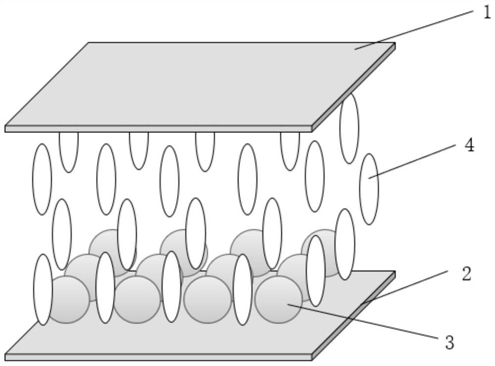
[0027] Embodiment 1: see figure 1 , a waveguide based on metamaterials, consisting of a metamaterial layer 3 wrapped by a liquid crystal 4 and upper and lower substrates 1, 2. The lowest layer is the lower substrate, which can be made of total reflection metal and other materials. The spherical superatoms are evenly distributed on the lower substrate at a fixed distance, and the superatoms are made of dielectric materials. The uppermost layer of the substrate can be made of materials such as total reflection metal, and the liquid crystal is filled between the upper and lower substrates and wraps the superatoms.
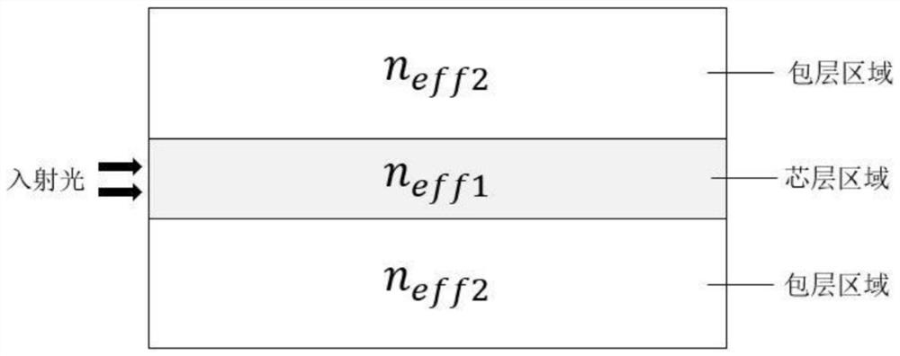
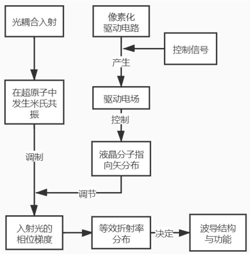
[0028] A waveguide works as follows. Such as figure 2 As shown, the waveguide is divided into a core region and a cladding region. Through the liquid crystal alignment technology, the liquid crystals in the core layer and the cladding area are set to have a specific director distribution, that is, the director distributions of the liquid crystal molecules in the c...
Embodiment 2
[0031] Embodiment 2: as figure 1 As shown, a tunable active waveguide based on metamaterial, the waveguide is composed of a metamaterial layer wrapped by liquid crystal and upper and lower substrates. Spherical superatoms with the same size are evenly distributed on the lower substrate at a fixed distance, and the superatoms are made of dielectric materials. The upper substrate is made of total reflection metal material, and the liquid crystal is filled between the upper and lower substrates and wraps the superatoms.
[0032] The lower substrate is a silicon-based pixelated control circuit, and each pixel controls the liquid crystal above it. After receiving the control signal, the circuit can make each pixel generate a driving electric field in the liquid crystal layer above it, and the driving electric field can control the director of the liquid crystal molecules in the pixel. Among them, the control mode of the liquid crystal adopts the FFS control mode. The initial dir...
Embodiment 3
[0036] Embodiment 3: as figure 1 As shown, a tunable active waveguide based on metamaterial, the waveguide is composed of a metamaterial layer wrapped by liquid crystal and upper and lower substrates. Spherical superatoms with the same size are evenly distributed on the lower substrate at a fixed distance, and the superatoms are made of dielectric materials. The upper substrate is made of total reflection metal material, and the liquid crystal is filled between the upper and lower substrates and wraps the superatoms.
[0037] The lower substrate is a silicon-based pixelated control circuit, and each pixel controls the liquid crystal above it. After receiving the control signal, the circuit can make each pixel generate a driving electric field in the liquid crystal layer above it, and the driving electric field can control the director of the liquid crystal molecules in the pixel. Among them, the control mode of liquid crystal adopts VA control mode. The initial director dis...
PUM
 Abstract
Description
Claims
Application Information
 - R&D
- Intellectual Property
- Life Sciences
- Materials
- Tech Scout
- Unparalleled Data Quality
- Higher Quality Content
- 60% Fewer Hallucinations
Browse by: Latest US Patents, China's latest patents, Technical Efficacy Thesaurus, Application Domain, Technology Topic, Popular Technical Reports.
© 2025 PatSnap. All rights reserved.Legal|Privacy policy|Modern Slavery Act Transparency Statement|Sitemap|About US| Contact US: help@patsnap.com