Super-junction insulated gate bipolar transistor structure and manufacturing method thereof

A technology of bipolar transistors and super junctions, applied in semiconductor/solid-state device manufacturing, semiconductor devices, electrical components, etc., can solve the problem of low conduction efficiency

Pending Publication Date: 2020-10-20
KUNSHAN HUATAI ELECTRONICS TECH CO LTD
View PDF5 Cites 0 Cited by
  • Summary
  • Abstract
  • Description
  • Claims
  • Application Information

AI Technical Summary

Problems solved by technology

[0002] The structure of a super junction insulated gate bipolar transistor in the current prior art is as follows figure 1 As shown, 1 is the P-collector region, 2 is the N-drift region, 3 is the P-type super junction region or P-type super junction structure, 4 is the N+ drift region, 5 is the gate oxide layer, and 6 is the gate , 7 is the P well region, 8 is the N+ emitter, 9 is the dielectric layer, 10 is the emitter metal, 11 is the P+ collector, 12 is the collector metal, the P in the existing super junction insulated gate bipolar transistor The region of the type super junction is on the same vertical line in the longitudinal direction. This structure is the same as that of the super junction VDMOSFET device. However, for the super junction VDMOSFET, there is only one kind of conductive carrier, such as an N-channel VDMOSFET Only electrons conduct electricity. In this case, electrons can pass through the middle of the P-type super junction region; but for super junction insulated gate bipolar transistors, there are two types of conductive carriers, both electrons and holes participate in conduction , such as N-channel insulated gate bipolar transistors, electrons from top to bottom and holes from bottom to top must pass through the entire N-drift region to complete recombination. Therefore, the existing super junction insulated gate bipolar transistor The conduction efficiency of the transistor is very low

Method used


Image

  • Super-junction insulated gate bipolar transistor structure and manufacturing method thereof
  • Super-junction insulated gate bipolar transistor structure and manufacturing method thereof

Examples


Embodiment 1

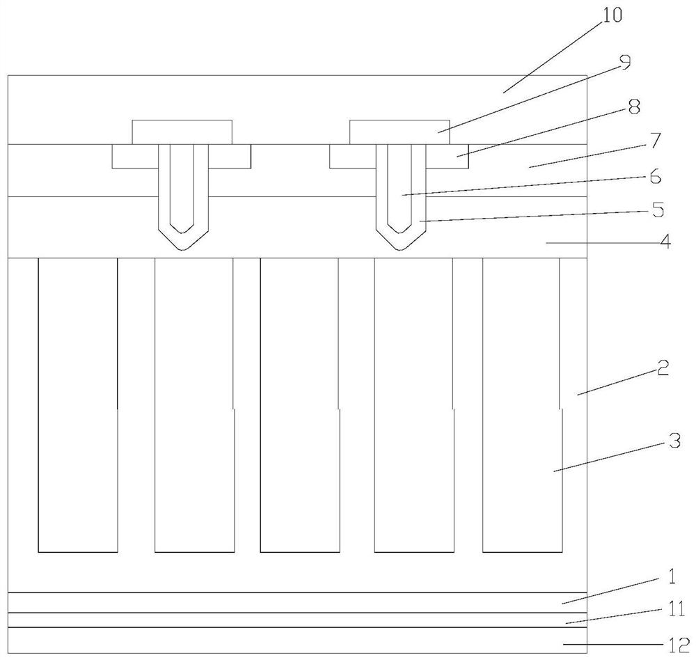
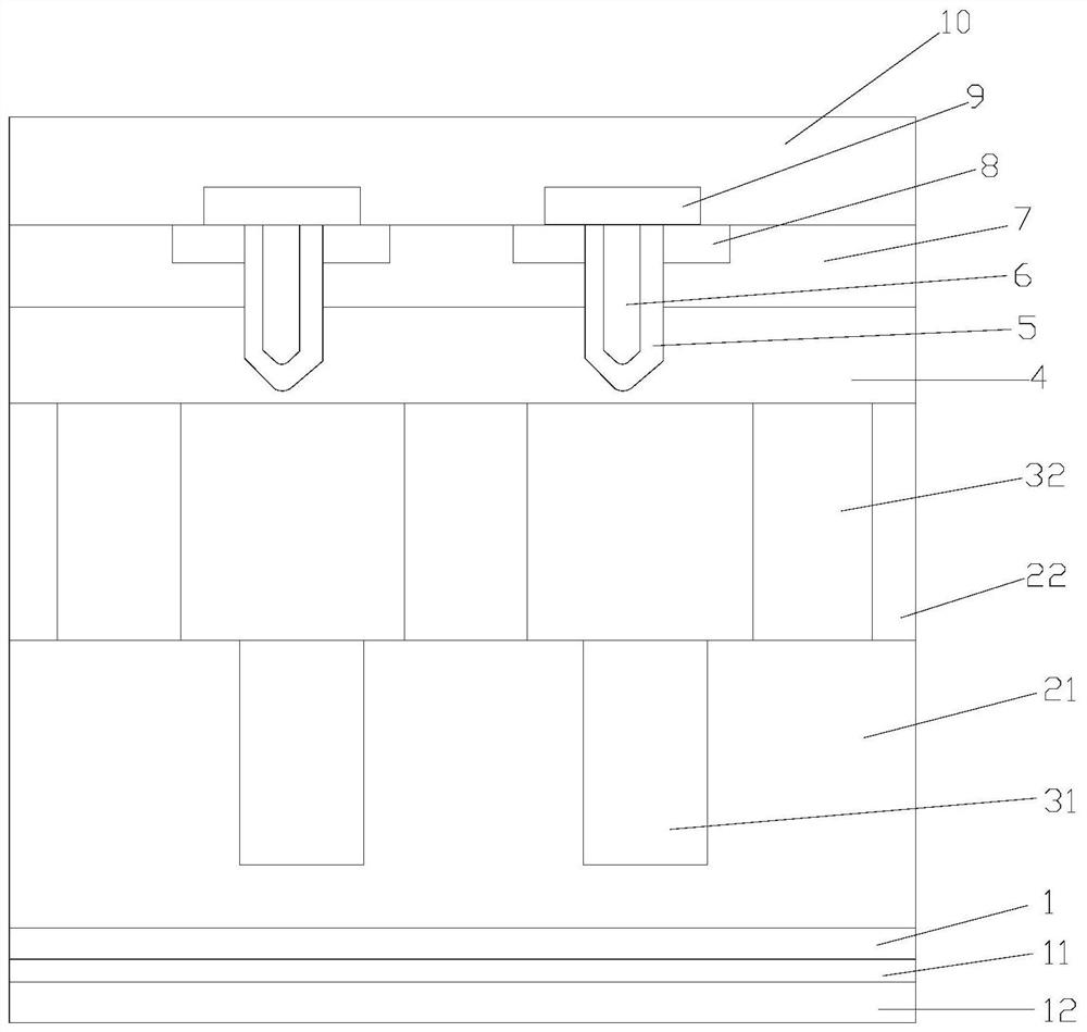
[0049] see figure 2 , a super junction insulated gate bipolar transistor structure, which includes a collector metal 12, a P+ collector 11, a P-collector region 1, a first N-drift region 21, a second N - drift region 22, N+ drift region 4, P well region 7 and emitter metal 10;

[0050] A plurality of first P-type super junctions 31 arranged at intervals are distributed in the first N-drift region 21, and a plurality of second P-type pillars 32 arranged at intervals are distributed in the second N-drift region 22, each A first P-type column 31 corresponds to at least one second P-type column 32 and forms a P-type super junction structure, and the first P-type column 31 and the second P-type column 32 are in the second direction Staggered from each other, the first P-type column 31 is also in contact with or connected to the second N-drift region 22, and the second P-type column 32 is also in contact with the first N-drift region 21 and the N+ drift region 4 respectively. or ...


PUM


Abstract

The invention discloses a super-junction insulated gate bipolar transistor structure and a manufacturing method thereof. The super-junction insulated gate bipolar transistor structure comprises a collector region, a first epitaxial layer and a second epitaxial layer which are sequentially arranged along a first direction. The collector region is matched with a collector; a plurality of super junction structures are distributed in the first epitaxial layer at intervals, each super junction structure comprises more than two super junctions which are sequentially arranged along a first direction,and the more than two super junctions are mutually staggered in a second direction; a plurality of first grooves are distributed in the second epitaxial layer at intervals, and a grid electrode is arranged in each first groove. According to the super-junction insulated gate bipolar transistor structure provided by the embodiment of the invention, the saturation voltage drop during conduction canbe reduced, and the super-junction insulated gate bipolar transistor structure provided by the embodiment of the invention can be used for accelerating the compounding of holes in a drift region whena device is turned off, reducing trailing current and reducing turn-off loss.

Description

technical field [0001] The invention relates to a transistor, in particular to a super junction insulated gate bipolar transistor structure and a manufacturing method thereof, which belong to the technical field of semiconductors. Background technique [0002] The structure of a super junction insulated gate bipolar transistor in the current prior art is as follows figure 1 As shown, 1 is the P-collector region, 2 is the N-drift region, 3 is the P-type super junction region or P-type super junction structure, 4 is the N+ drift region, 5 is the gate oxide layer, and 6 is the gate , 7 is the P well region, 8 is the N+ emitter, 9 is the dielectric layer, 10 is the emitter metal, 11 is the P+ collector, 12 is the collector metal, the P in the existing super junction insulated gate bipolar transistor The region of the type super junction is on the same vertical line in the longitudinal direction. This structure is the same as that of the super junction VDMOSFET device. However, ...

Claims


Application Information

Patent Timeline
Patent Type & Authority Applications(China)
IPC IPC(8): H01L29/06H01L29/739H01L21/331
CPCH01L29/7398H01L29/7397H01L29/66348H01L29/0634H01L29/0684
Inventor 卢烁今
Owner KUNSHAN HUATAI ELECTRONICS TECH CO LTD
Why Eureka
Try Eureka