Conductive film with low b * value and high transmittance
A high transmittance, conductive film technology, applied in the field of conductive film, can solve the problems of damaging the conductivity and transparency of the conductive film, and achieve the effect of suppressing the decrease in transparency, high transmittance, and improving scratch resistance.
- Summary
- Abstract
- Description
- Claims
- Application Information
AI Technical Summary
Problems solved by technology
Method used
Image
Examples
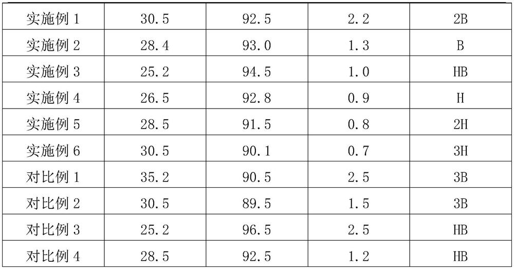
Embodiment 1
[0031] The conductive film with low b* value and high transmittance in this embodiment is prepared by the following method:
[0032] (1) Hollow SiO 2 Preparation of microspheres: First, 2.5 g of cetyltrimethylammonium bromide (CTAB) was added into deionized water at 60° C., and ultrasonically dispersed and dissolved. Then add 6 mL of n-hexadecane, and stir at 800 rpm for 10 min to form an O / W emulsion system. Add 20mL concentrated ammonia water, keep stirring at 60°C for 30min, then add 20mL tetraethyl orthosilicate (TEOS) and 1.0g polyvinyl alcohol (PVA) dropwise, and continue stirring for 6h to fully mix. After cooling to room temperature, wash three times with absolute ethanol and deionized water, and dry in vacuum for 24 h to obtain hollow SiO 2 Microspheres.
[0033] (2) Hollow SiO 2 Staining of microspheres: First, weigh 0.5g of blue dye and dissolve it in 20ml of absolute ethanol, then weigh 50g of hollow SiO 2 Under the condition of magnetic stirring, slowly add t...
Embodiment 2
[0037] The preparation method of the conductive film of this example is basically the same as that of Example 1, the only difference is that the blue hollow SiO with a mass fraction of 0.3wt% is used 2 Microspheres were added to the silver nanowire conductive ink.
Embodiment 3
[0039] The preparation method of the conductive film of this example is basically the same as that of Example 1, the only difference is that the blue hollow SiO with a mass fraction of 0.5wt% 2 Microspheres were added to the silver nanowire conductive ink.
PUM
| Property | Measurement | Unit |
|---|---|---|
| diameter | aaaaa | aaaaa |
| refractive index | aaaaa | aaaaa |
| aspect ratio | aaaaa | aaaaa |
Abstract
Description
Claims
Application Information
 - R&D Engineer
- R&D Manager
- IP Professional
- Industry Leading Data Capabilities
- Powerful AI technology
- Patent DNA Extraction
Browse by: Latest US Patents, China's latest patents, Technical Efficacy Thesaurus, Application Domain, Technology Topic, Popular Technical Reports.
© 2024 PatSnap. All rights reserved.Legal|Privacy policy|Modern Slavery Act Transparency Statement|Sitemap|About US| Contact US: help@patsnap.com


