Base plate and packaging structure

A substrate and substrate surface technology, applied in semiconductor/solid-state device components, semiconductor devices, electrical components, etc., can solve problems such as product failure, large substrate warpage, and semiconductor product damage, and avoid delamination of packaging glue and substrate , Guarantee the placement quality, and suppress the effect of substrate warpage

Inactive Publication Date: 2020-10-02
SUZHOU TF AMD SEMICON CO LTD
View PDF3 Cites 0 Cited by
  • Summary
  • Abstract
  • Description
  • Claims
  • Application Information

AI Technical Summary

Problems solved by technology

[0002] In the manufacturing process of semiconductor products, the packaging process is required. In the packaging process of existing products, especially in the high temperature process, the warpage of the substrate is large, which leads to the damage of semiconductor products:
[0003] 1. The warpage of the substrate in the reflow oven will cause damage to the solder layer and eventually lead to product failure;
[0004] 2. During the curing process of the encapsulant, the warping of the substrate will lead to delamination of the encapsulant and the product, and eventually lead to product failure;
[0005] 3. During the process of mounting the heat dissipation cover and metal heat sink or the curing of the thermal conductive adhesive, the warping of the substrate leads to voids or delamination of the metal layer, which eventually leads to product damage and failure

Method used


Image

  • Base plate and packaging structure
  • Base plate and packaging structure
  • Base plate and packaging structure

Examples


Embodiment Construction

[0026] The application will be further described in detail below with reference to the drawings and embodiments. It can be understood that the specific embodiments described here are only used to explain the related invention, but not to limit the invention. In addition, it should be noted that, for ease of description, only the parts related to the invention are shown in the drawings.

[0027] It should be noted that the embodiments in the application and the features in the embodiments can be combined with each other if there is no conflict. Hereinafter, the present application will be described in detail with reference to the drawings and in conjunction with embodiments.

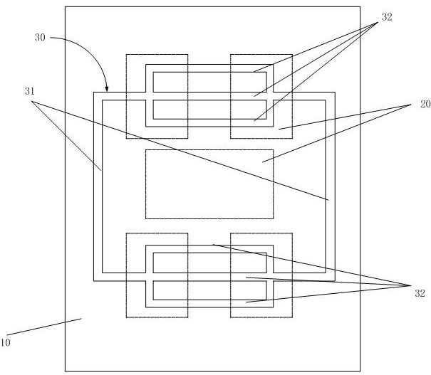
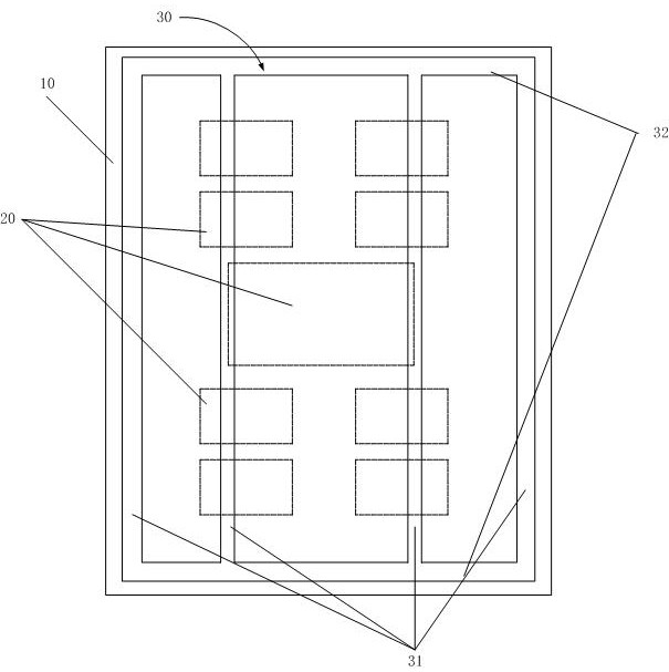
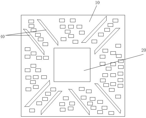
[0028] reference Figure 5 The package structure includes a substrate 100 and a chip 200 and passive components arranged on the substrate carrying surface. The substrate 100 has an interconnected metal conductive layer, and the conductive layer connecting the chip 200 and the passive component is exposed on ...


PUM


Abstract

The invention provides a base plate and a packaging structure. The base plate comprises: a substrate internally provided with a first reinforcing part for inhibiting the warping of the base plate; or / and a second reinforcing part used for inhibiting the warping of the base plate and arranged on the surface of the base plate. According to the invention, by arranging the first reinforcing part or / and the second reinforcing part, the purpose of inhibiting warping of the base plate is achieved, so that the warping of the base plate can be inhibited when the packaging structure is used for packaging or reflow soldering, solder ball damage for connecting a chip and the base plate and delamination of packaging glue and the base plate are avoided, the reliability of a product is improved, and theyield of the product is increased.

Description

Technical field [0001] The present invention generally relates to the field of semiconductor manufacturing, in particular to a substrate and packaging structure. Background technique [0002] In the manufacturing process of semiconductor products, it is necessary to go through the packaging process. In the packaging process of existing products, especially in the high temperature process, the warpage of the substrate is large, which leads to the damage of the semiconductor product: [0003] 1. The warpage of the substrate in the reflow oven will cause damage to the solder layer and ultimately lead to product failure; [0004] 2. In the process of curing the packaging glue, the substrate warping will cause the packaging glue and the product to delamination, which will eventually lead to the product failure; [0005] 3. During the curing process of mounting the heat sink cover and the metal heat sink or the thermal conductive adhesive, the substrate warps and causes the metal layer to b...

Claims


Application Information

Patent Timeline
Patent Type & Authority Applications(China)
IPC IPC(8): H01L23/498
CPCH01L23/49827H01L23/49838
Inventor 周云
Owner SUZHOU TF AMD SEMICON CO LTD
Why Eureka
Try Eureka