
Substrate, semiconductor device and manufacturing method of semiconductor device

A manufacturing method and semiconductor technology, applied in the field of semiconductors, can solve problems such as semiconductor device degradation, lattice mismatch, and unfavorable crystal quality of semiconductor devices, so as to improve performance and reliability, reduce lattice mismatch rate, and improve mechanical strength Effect

Inactive Publication Date: 2020-09-25
度亘核芯光电技术(苏州)有限公司
View PDF6 Cites 0 Cited by
  • Summary
  • Abstract
  • Description
  • Claims
  • Application Information

AI Technical Summary

Problems solved by technology

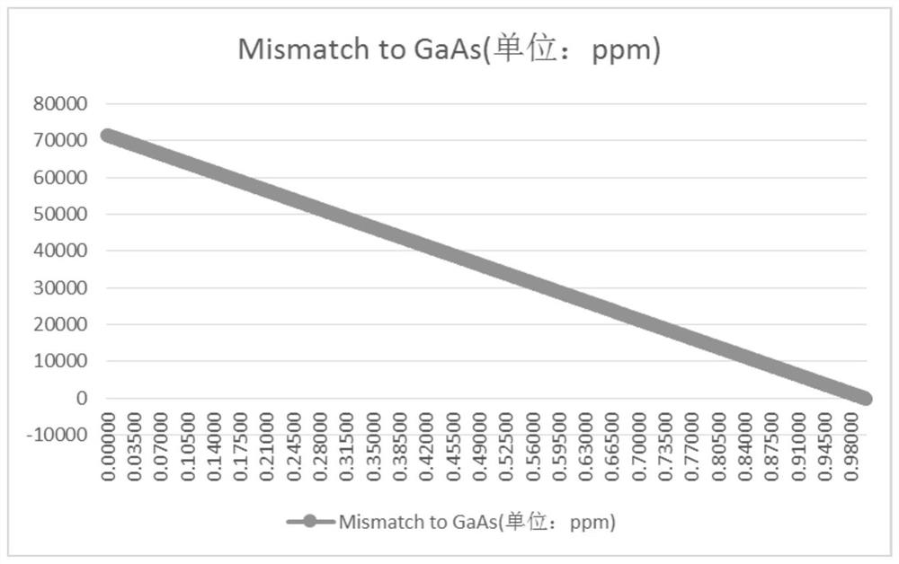
[0003] In the prior art, the common lasing wavelength is 1064nm laser, which includes InGaAs / GaAs strained quantum well, and GaAs substrate, and it requires the active region InGaAs to contain about 30% In composition, high composition In The lattice mismatch between the active region and the substrate can reach 2%-3%, and it is easy to introduce dislocations and various defects due to stress release, leading to the degradation of semiconductor devices. Among them, the greater the amount of In composition, the mismatch or greater stress
[0004] In the prior art, some large-strain quantum well materials are obtained by cooling the growth method, but the cooling growth is not good for the crystal quality of the semiconductor device itself, and the crystal of the semiconductor device is prone to defects, which will affect the migration of electrons and the semiconductor device. Lifetime, there are defects in the direction from the production point of view
In the prior art, some methods use strain compensation, but it has a negative impact on the treatment of the interface and the luminous efficiency of the quantum well. From the perspective of production, there are defects

Method used


Image

  • Substrate, semiconductor device and manufacturing method of semiconductor device
  • Substrate, semiconductor device and manufacturing method of semiconductor device
  • Substrate, semiconductor device and manufacturing method of semiconductor device

Examples


Embodiment Construction

[0047] The terms "first", "second", "third" and so on are only used for distinguishing descriptions, and do not represent sequence numbers, nor can they be understood as indicating or implying relative importance.

[0048]In addition, the terms "horizontal", "vertical", "overhanging" and the like do not mean that the components are absolutely horizontal or overhanging, but may be slightly inclined. For example, "horizontal" only means that its direction is more horizontal than "vertical", and it does not mean that the structure must be completely horizontal, but can be slightly inclined.

[0049] In the description of the present application, it should be noted that the orientation or positional relationship indicated by the terms "inner", "outer", "left", "right", "upper", "lower" etc. are based on the Orientation or positional relationship, or the orientation or positional relationship that the application product is usually placed in use, is only for the convenience of desc...


PUM


Abstract

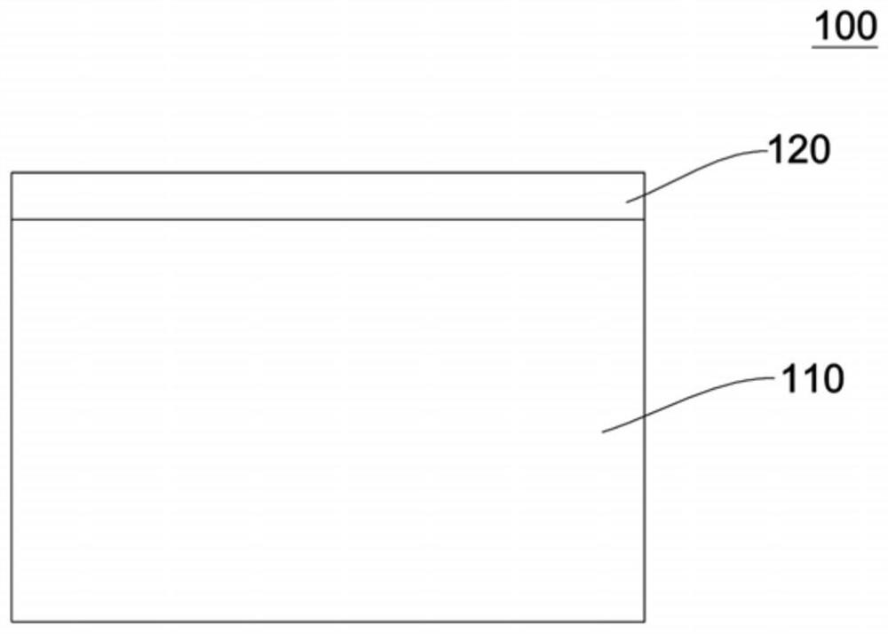
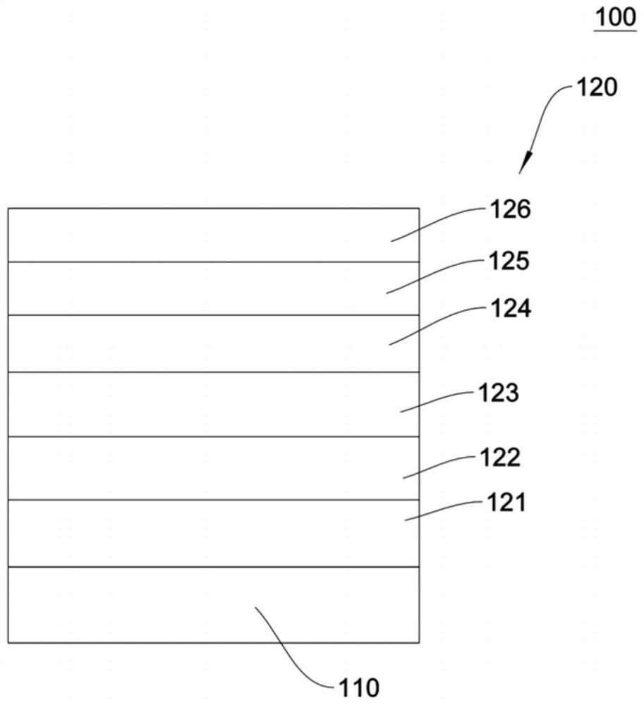
The invention discloses a substrate, a semiconductor device and a manufacturing method of the semiconductor device, and belongs to the technical field of semiconductors. The material of the substrateis InxGa1-xAs, wherein x is greater than 0 and less than 1. According to the substrate, the semiconductor device and the manufacturing method of the semiconductor device of the invention, the In element is added into the substrate, so that the mechanical strength of the substrate is improved, the lattice constant of the InGaAs material in the quantum well of an active region is close to that of the substrate, so that the lattice mismatch rate of the active region and the substrate is reduced; and the stress of an epitaxial wafer can be effectively reduced, the quality of the semiconductor device is improved, and the performance and reliability of the semiconductor device are improved.

Description

technical field [0001] The present application relates to the technical field of semiconductors, and in particular, to a substrate, a semiconductor device, and a method for manufacturing the semiconductor device. Background technique [0002] 1064nm band laser is widely used in military fields such as ranging, guidance and jamming, as well as high-tech fields such as coherent communication, atmospheric research, medical equipment, optical image processing, and laser printers. The InGaAs / GaAs strained quantum well laser with a lasing wavelength of 1064nm can be used in some aspects such as handheld laser ranging, mortar launchers, etc. due to its small size, high photoelectric conversion efficiency, convenient modulation, and low price. It becomes a more suitable laser light source instead of the original solid-state laser. [0003] In the prior art, the common lasing wavelength is 1064nm laser, which includes InGaAs / GaAs strained quantum well, and GaAs substrate, and it req...

Claims


Application Information

Patent Timeline
Patent Type & Authority Applications(China)
IPC IPC(8): H01S5/02H01S5/343
CPCH01S5/0211H01S5/34313
Inventor 杨国文赵勇明杨皓宇赵卫东
Owner 度亘核芯光电技术(苏州)有限公司
Learn More