


Quick Research
Generate reliable direction feasibility study reports for your R&D in just a few steps.

Technical Q&A
Discover and master advanced knowledge NOW. Basics, ideas, possibilities, all at once.

Find Solutions
As an expert in R&D theories, this can generate solutions to your technical problems instantly.

Evaluate Feasibility
Analyze your overall solution with one click, know your potential R&D risks in advance.

Monitor Landscape
Get weekly tech updates, stay abreast of the latest tech innovations and key insights.
Method for preparing graphene single crystal wafer on copper-based textured thin film substrate
A graphene and single crystal technology, which is applied in the field of preparing graphene single crystal wafers on copper-based textured film substrates, can solve problems such as high costs, and achieve the effects of reducing production costs, achieving wide application and consistent orientation.
- Summary
- Abstract
- Description
- Claims
- Application Information
AI Technical Summary
Problems solved by technology
Method used
Image


Examples
Embodiment 1
[0032] Using the magnetron sputtering method to deposit 800nm copper-based textured film on the surface of sapphire at room temperature, in which copper is the main element, nickel is the auxiliary element, and the content of nickel element is 15%, realizing the copper-based textured film substrate. preparation. Then, the copper-based textured film substrate is placed in a chemical vapor deposition system, and annealed in an argon and hydrogen protective atmosphere, the flow ratio of argon and hydrogen is 300sccm:80sccm, the annealing temperature is 1000°C, and the annealing time After 60 minutes, 10 sccm of methane was introduced, and the growth temperature of the graphene film was 1000°C for 10 minutes, so that a graphene single crystal wafer was epitaxially grown on the surface of the copper-based textured film substrate.
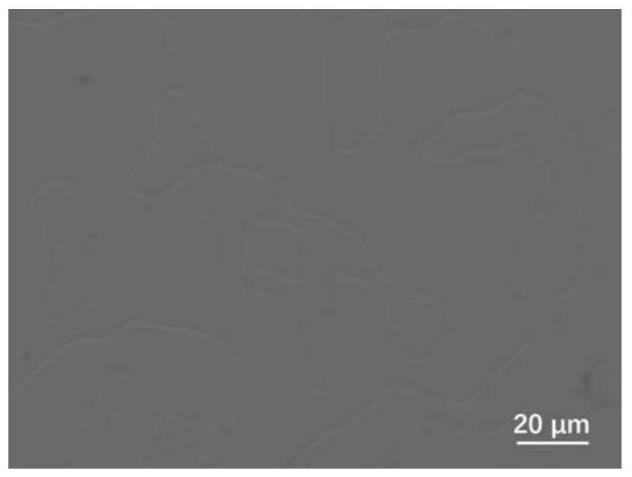
[0033] figure 1 It is the optical microscope topography of graphene on the surface of copper-based textured film. From the figure, it can be seen tha...
Embodiment 2
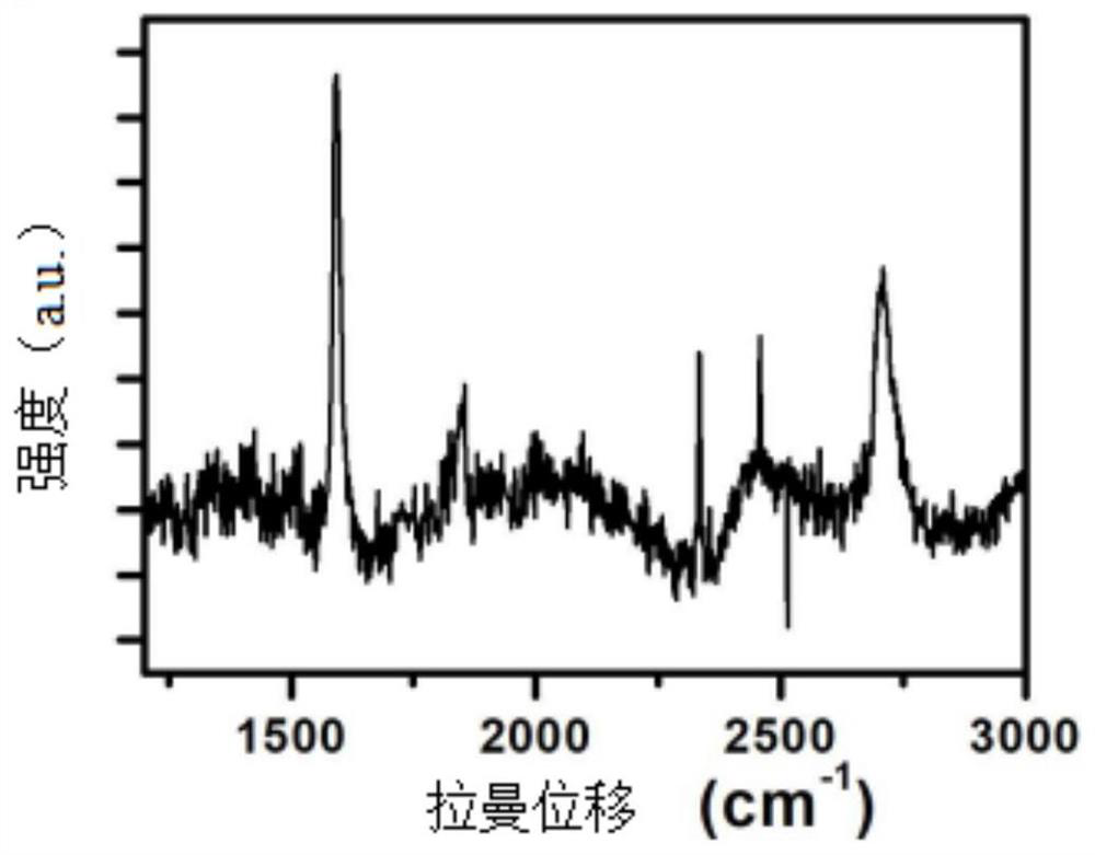
[0035] The difference between this example and Example 1 is that the content of nickel element in the copper-based textured film substrate prepared in Example 1 is adjusted from 15% to 10%, the flow ratio of argon and hydrogen is 200sccm:50sccm, annealing The temperature is 800° C., the annealing time is 100 minutes, the growth temperature of the graphene film is 300° C., and the rest of the process parameters are the same as in the first embodiment. Such as Figure 7 As shown, by analyzing the Raman spectrum inside the crystal domain, at ~1600cm -1 And ~ 2700cm -1 The characteristic peaks of graphene appear at , and the absence of defect peaks proves that the quality of the grown graphene is high. Such as Figure 8 As shown, the LEED diffraction spot of graphene on the surface of the copper-nickel alloy film in Example 2 shows that the orientation of graphene is consistent, and it is a single crystal film.
Embodiment 3
[0037] The difference between this embodiment and the first embodiment is that the content of the nickel element in the copper-based textured film substrate in the first embodiment is adjusted to 5%, the flow ratio of argon and hydrogen is 100 sccm:20 sccm, and the annealing temperature is 500°C. The annealing time was 120 minutes, the growth temperature of the graphene film was 500° C., and the rest of the process parameters were the same as in the first embodiment. Such as Figure 9 As shown, by analyzing the Raman spectrum inside the crystal domain, at ~1600cm -1 And ~ 2700cm -1 Graphene characteristic peaks appear at , and no defect peaks of graphene are observed, confirming that the quality of the grown graphene is higher; Figure 10 It is the LEED diffraction pattern of the graphene on the surface of the alloy textured film in this embodiment, and the result shows that the orientation of the graphene on the surface of the copper-nickel textured film is consistent, and ...
PUM
| Property | Measurement | Unit |
|---|---|---|
| thickness | aaaaa | aaaaa |
Abstract
Description
Claims
Application Information
 - R&D Engineer
- R&D Manager
- IP Professional
- Industry Leading Data Capabilities
- Powerful AI technology
- Patent DNA Extraction
Browse by: Latest US Patents, China's latest patents, Technical Efficacy Thesaurus, Application Domain, Technology Topic, Popular Technical Reports.
© 2024 PatSnap. All rights reserved.Legal|Privacy policy|Modern Slavery Act Transparency Statement|Sitemap|About US| Contact US: help@patsnap.com