Method for preparing patterned silicon structure and silicon-based photovoltaic cell

A patterned, silicon-structured technology, applied in photovoltaic power generation, circuits, electrical components, etc., can solve the problems of increasing the manufacturing cost of photovoltaic cells, limited anti-reflection performance, low contrast, etc., to improve photoelectric conversion efficiency and avoid viewing angles. Problem, effect of improving absorption rate

Active Publication Date: 2022-03-01
SUZHOU UNIV
View PDF5 Cites 0 Cited by
  • Summary
  • Abstract
  • Description
  • Claims
  • Application Information

AI Technical Summary

Problems solved by technology

[0004] In the prior art, such as the patent application with the application number CN201811354383.7, there is a method of using the silicon inverted pyramid structure to realize the pattern, but this method still has many key shortcomings, so that it is difficult to be applied: 1) Visible Small angle: The reflection of the wet-etched inverted pyramid is anisotropic. Both the (100) plane of the original silicon wafer and the (111) plane formed after etching are atomically flat crystal planes, which can achieve Specular reflection, resulting in the correct designed pattern etched on the silicon wafer can only be seen under the incidence of plane light and certain fixed viewing angles
2) Low contrast: The anti-reflection performance of the inverted pyramid structure is limited, resulting in a very low contrast ratio of the pattern obtained, which is only 5:1, which is also prone to gray bands formed by discontinuous grayscale transitions. At the same time, the inverted pyramid is weak The anti-reflection performance is also not conducive to the acquisition of high-efficiency photovoltaic cells
3) Complicated preparation process: Wet etching of inverted pyramid arrays generally requires a hard mask (SiO 2 ), and using photolithography and dry etching to pattern this mask, synthesis and processing of such hard masks will significantly increase the manufacturing cost of photovoltaic cells

Method used


Image

  • Method for preparing patterned silicon structure and silicon-based photovoltaic cell
  • Method for preparing patterned silicon structure and silicon-based photovoltaic cell
  • Method for preparing patterned silicon structure and silicon-based photovoltaic cell

Examples


preparation example Construction

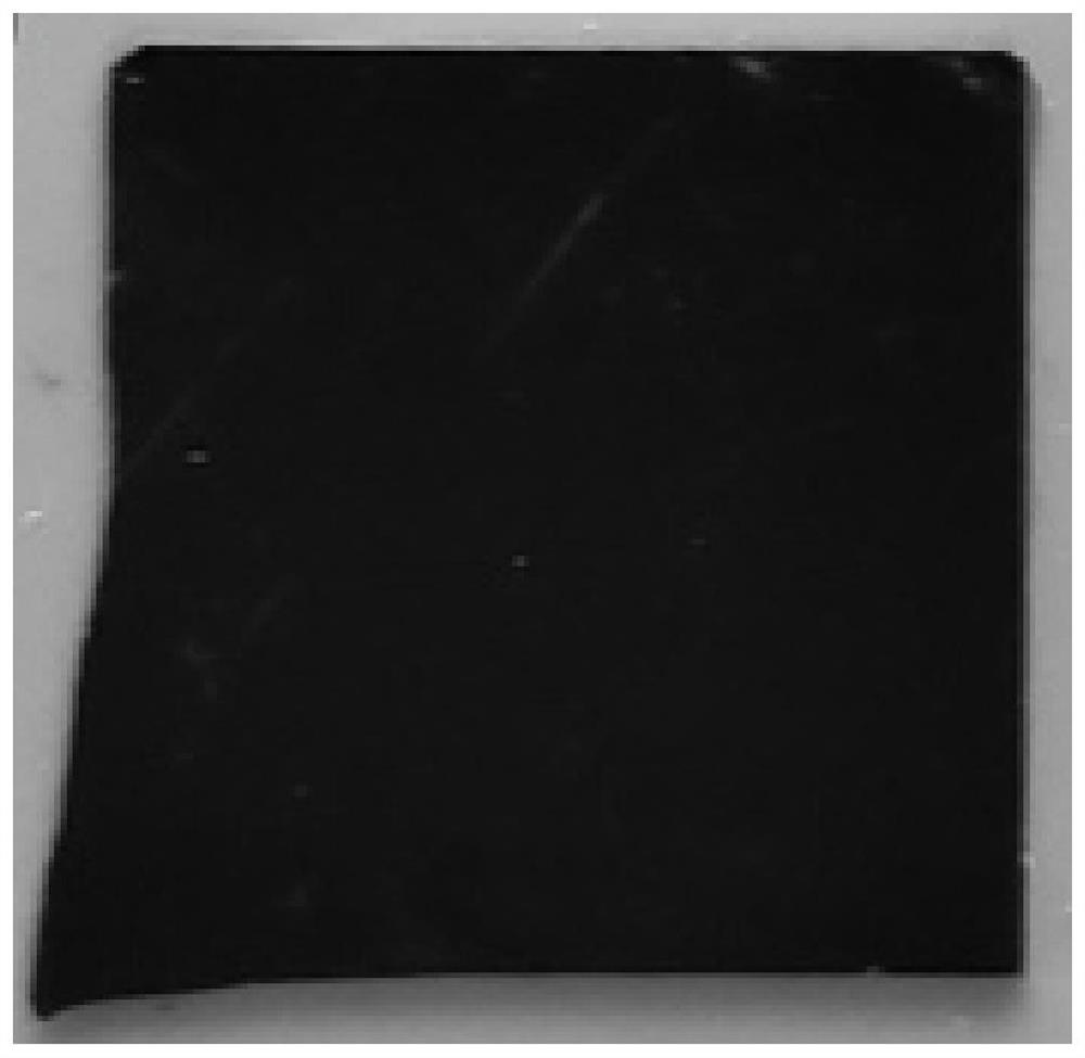
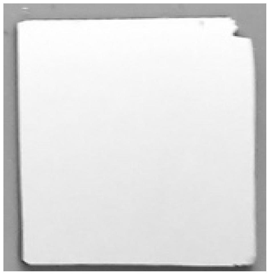
[0063] figure 1 A schematic flowchart of a method for fabricating a patterned silicon structure according to an embodiment of the present invention is shown. This preparation method is used to display a grayscale image on a non-polished silicon substrate, and the pattern displayed on the silicon substrate is composed of a plurality of pixels with different reflectivities, such as figure 1 Shown, this preparation method comprises:

[0064] Step S100, providing a non-polished silicon substrate and a grayscale image with a preset pattern;

[0065] Step S200, setting the pixel point array to be displayed on the silicon substrate according to the preset pattern, the pixel point array is composed of a plurality of pixels arranged according to the preset pattern and having the same size, and each pixel point is formed by the silicon substrate to be etched The region to be etched formed by the textured structure on the substrate and the unetched region of the textured structure not ...


PUM

PropertyMeasurementUnit
reflectanceaaaaaaaaaa

Abstract

The invention provides a method for preparing a patterned silicon structure and a silicon-based photovoltaic cell. The preparation method includes: providing a non-polished silicon substrate and a grayscale image with a preset pattern; setting an array of pixel points to be displayed on the silicon substrate according to the preset pattern, and each pixel point is formed by the silicon substrate to be etched The area to be etched formed by the textured structure on the substrate and the unetched area of ​​the unetched textured structure are composed according to a predetermined ratio; the size of the pixel point and the size of the pixel to be etched are determined according to the optical parameters of the silicon substrate and the textured structure. Which area in the etched area and the unetched area is used as the central area of ​​the pixel; obtain the relationship between the gray value of the grayscale image and the side length of the central area of ​​​​the pixel; convert the grayscale matrix of the grayscale image according to the conversion relationship It is a structural pattern composed of pixel point arrays to be displayed on the silicon substrate; using the structural pattern to produce a photolithographic mask; using the photolithographic mask to etch a pattern corresponding to the grayscale image on the silicon substrate according to the patterning process.

Description

technical field [0001] The invention relates to the field of semiconductor devices, in particular to a method for preparing a patterned silicon structure and a silicon-based photovoltaic cell. Background technique [0002] The most important energy consumption in human society is industrial energy consumption, transportation energy consumption and building energy consumption. With the increase of population and the development of urbanization, building energy consumption has surpassed industrial energy consumption and transportation energy consumption, and occupies the first place in social energy consumption. Therefore, the concept of "low energy building" was put forward. Combining photovoltaics with buildings gives full play to the advantages of photovoltaic energy and equipment, low energy loss, no environmental pollution, and easy integration with building structures. Architectural designers integrate photovoltaic devices into architectural design, and specific applic...

Claims


Application Information

Patent Timeline
Patent Type & Authority Patents(China)
IPC IPC(8): H01L31/0236H01L31/18H01L31/028H01L31/06
CPCH01L31/02363H01L31/1804H01L31/028H01L31/06Y02E10/547Y02P70/50
Inventor 揭建胜张晓宏丁可
Owner SUZHOU UNIV
Why Eureka
Try Eureka